Cleaning method and cleaning apparatus for performing the same

a cleaning method and cleaning method technology, applied in the direction of cleaning process and apparatus, cleaning using liquids, cleaning methods, etc., can solve the problems of lowering the yield and productivity of the semiconductor device, batch cleaning methods may not effectively clean the edge and side sections of the semiconductor substrate, and the cleaning method may not effectively remove the impurities sticking to the side and bottom sections of the semiconductor substrate. , to achieve the effect of improving the cleaning effect and improving the cleaning effect with respect to the edge and side sections of the semiconductor

Inactive Publication Date: 2006-04-13
SAMSUNG ELECTRONICS CO LTD
View PDF11 Cites 9 Cited by
  • Summary
  • Abstract
  • Description
  • Claims
  • Application Information

AI Technical Summary

Benefits of technology

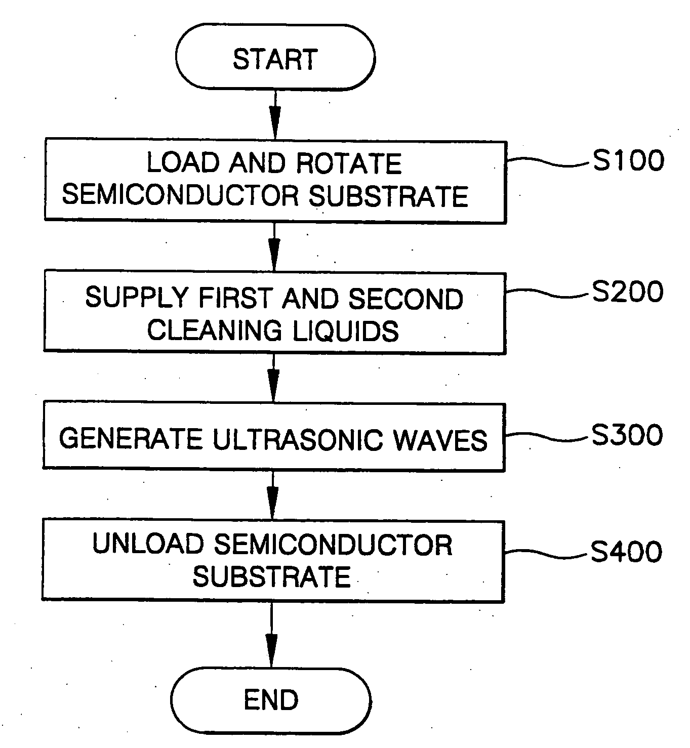
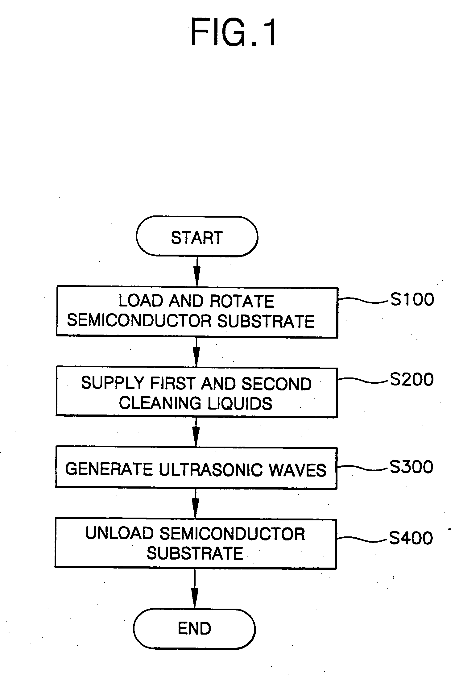
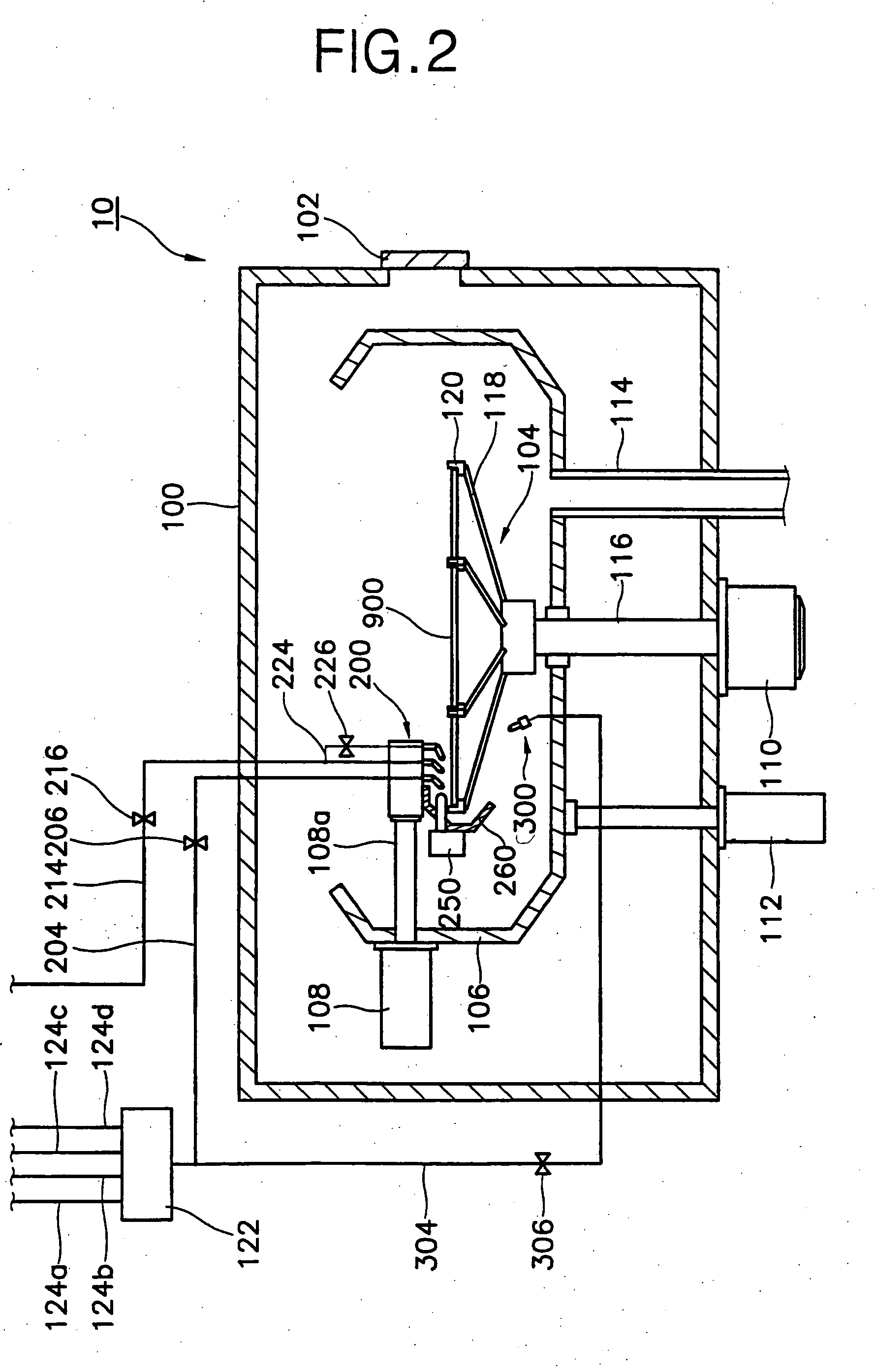
[0009] Embodiments of the present invention provide cleaning apparatus and methods that can effectively remove impurities from edge, side and bottom sections of a semiconductor substrate while preventing cleaning liquid from penetrating into a center portion of the semiconductor substrate.
[0012] The cleaning liquid supplied from the upper nozzle may flow from the edge section to the side section of the semiconductor substrate, and the ultrasonic waves may be applied to the cleaning liquid supplied to the edge section. In this manner, the cleaning effect with respect to the edge and side sections of the semiconductor substrate can be improved.
[0013] In addition, first and second nitrogen gas streams may be supplied from further respective nozzles to prevent the cleaning liquid from moving into the center portion of the semiconductor substrate. Accordingly, a pattern and a metal wiring formed on the semiconductor substrate can be protected from the cleaning liquid.
[0014] In addition, a further nozzle may be provided to supply a second cleaning liquid to a bottom section of the semiconductor substrate. The ultrasonic waves generated from the ultrasonic wave generator may be applied to the second cleaning liquid supplied to the bottom section by passing through the semiconductor substrate to improve the cleaning effect with respect to the bottom section.

Problems solved by technology

However, impurities that remain at an edge section, a side section and a bottom section of the semiconductor substrate while the unit processes are being carried out typically are not completely removed through a general cleaning process.
However, the single-wafer type cleaning method may not effectively remove the impurities sticking to the side and bottom sections of the semiconductor substrate.
Furthermore, the batch type cleaning method may not effectively clean the edge and side sections of the semiconductor substrate.
The impurities sticking to the surface of the semiconductor substrate may ca use a process failure when performing a following process, thereby lowering the yield and productivity of the semiconductor device.
In addition, because the photolithography process is required for protecting the metal wiring during the cleaning process, the manufacturing cost of the semiconductor device is increased.
However, Kuniyasu's cleaning device does not selectively clean a specific portion of the wafer.
However, the cleaning devices of the U.S. patents may cause a center portion of the wafer formed with a metal wiring to be exposed to the cleaning liquid.

Method used


Image

  • Cleaning method and cleaning apparatus for performing the same
  • Cleaning method and cleaning apparatus for performing the same
  • Cleaning method and cleaning apparatus for performing the same

Examples


example

[0064] Table 1 shows test results of cleaning efficiency with respect to the semiconductor substrate. The tests were carried out with applying the ultrasonic waves to SC1 solution and without applying the ultrasonic waves to general SC1 solution.

TABLE 1Power3060usedsecsecSC1 (without ultrasonic wave)031.0%35.0%SC1 (both surfaces of substrate) +5099.7%99.3%ultrasonic wave (upper surface of7581.4%92.5%substrate10084.8%93.1%12585.4%95.8%Deionized water (upper surface of5098.7%—Frontsubstrate) + SC1 (lower surface ofloadingsubstrate) + ultrasonic wave5099.7%—Bottom(upper surface of substrateloading

[0065] In the above test, the semiconductor substrate was intentionally contaminated with silicon nitride (SiN) gel, and the silicon nitride gel was removed by using SC1 solution having a temperature of about 65° C. The frequency of the ultrasonic wave was 830 kHz.

[0066] In the first test, the semiconductor substrate was loaded such that a surface formed with the silicon nitride gel was upw...


PUM

PropertyMeasurementUnit
incident angleaaaaaaaaaa
distanceaaaaaaaaaa

Abstract

A cleaning apparatus includes upper and lower nozzle assemblies supplying a cleaning liquid to edge and bottom sections of a semiconductor substrate. The upper nozzle assembly has a first nozzle supplying the cleaning liquid onto the edge section, and second and third nozzles supplying a nitrogen gas for preventing the cleaning liquid from moving into a center portion of the semiconductor substrate. The cleaning liquid supplied to the edge section flows from the edge section towards a side section of the semiconductor substrate due to the rotation of the semiconductor substrate. An ultrasonic wave generator is provided above the edge section for generating ultrasonic waves. The ultrasonic waves are applied to the cleaning liquid supplied onto the edge and bottom sections, thereby improving the cleaning efficiency. The cleaning apparatus has a guide to guide the cleaning liquid supplied to the edge section toward the side section. The cleaning apparatus may effectively remove impurities from the edge, side and bottom sections of the semiconductor substrate.

Description

RELATED APPLICATIONS [0001] The present application claims priority from Korean Patent Application No. 2001-74311, filed Nov. 27, 2001, the disclosure of which is hereby incorporated herein by reference in its entirety. FIELD OF THE INVENTION [0002] The present invention relates to methods and apparatus for cleaning semiconductor substrates and, more particularly, to a method and an apparatus for cleaning an edge section, a side section, and a bottom section of a semiconductor substrate. BACKGROUND OF THE INVENTION [0003] Generally, semiconductor devices are manufactured by sequentially performing unit processes, such as deposition, photolithography, etching, ion implantation, polishing, cleaning and drying processes, on a semiconductor substrate. Among the above unit processes, the cleaning process is carried out after each unit process has been finished so as to remove the residue remaining on the semiconductor substrate. Recently, as designs tend to require a micro-sized pattern,...

Claims


Application Information

Patent Timeline
Patent Type & Authority Applications(United States)
IPC IPC(8): B08B3/12C03C23/00B08B3/00H01L21/304H01L21/00H01L21/02
CPCB08B3/12H01L21/02052H01L21/67051Y10S134/902H01L21/304
Inventor NAM, CHANG-HYEONSON, HONG-SEONGKIM, KYUNG-HYUN
Owner SAMSUNG ELECTRONICS CO LTD
Why Eureka
Try Eureka