Electronic device and method for fabricating the same

a technology of electronic devices and manufacturing methods, applied in semiconductor devices, semiconductor/solid-state device details, electrical apparatus, etc., can solve the problems of insulating films with a low dielectric constant, defective products, cracks or flaws in parts of seal rings, etc., to prevent the degradation of moisture resistance and reliability of semiconductor chips

Active Publication Date: 2006-04-13
PANNOVA SEMIC
View PDF8 Cites 63 Cited by
  • Summary
  • Abstract
  • Description
  • Claims
  • Application Information

AI Technical Summary

Benefits of technology

[0028] Since the characteristic features of the present invention described above allow a crack, flaw, or the like caused by dicing in the wafer when the individual chips (semiconductor devices) are collected from the wafer to be blocked by the stress absorbing wall or walls in a single, double, or higher-order multiple structure before it reaches the seal ring, the destruction of the seal ring and the resulting destruction of the chip region serving as the semiconductor device can be presented. As a result, it becomes possible to prevent the degradation of the moisture resistance and reliability of the semiconductor chip.
[0029] Thus, the present invention relates to an electronic device having a seal ring formed to surround the chip region and a mechanism for protecting the seal ring and is extremely useful since it achieves the effect of allowing the seal ring to retain the function of reliably protecting the inner portion of the chip region by blocking a crack, stress, or the like that has occurred during dicing by using a stress absorbing wall.

Problems solved by technology

In the conventional semiconductor device, however, even though a crack or impact that has occurred during the dicing of a wafer can be prevented from propagating toward the inner portion of the chip region by using the seal ring, a crack or flaw occurs in a part of the seal ring.
When packaging is performed with respect to the semiconductor device in such a condition, the residue of the seal ring comes into contact with a bonding wire and causes a defective product.
However, since the interlayer insulating film with a low dielectric constant is typically low in mechanical strength, the resistance of the interlayer insulating film with a low dielectric constant to a stress occurring during dicing is less sufficient than the resistance of a material that has been used conventionally for an interlayer insulating film.
Accordingly, the interlayer insulating film with a low dielectric constant is more susceptible to damage during dicing.
As a result, it has been becoming increasingly difficult to perform both of the function of preventing the propagation of a crack or the like that has occurred during dicing and the function of preventing the ingression of moisture, movable ions, and the like into the chip region from the outside thereof by using only a seal ring, as has been performed conventionally.

Method used


Image

  • Electronic device and method for fabricating the same
  • Electronic device and method for fabricating the same
  • Electronic device and method for fabricating the same

Examples


embodiment 1

[0067] An electronic device according to a first embodiment of the present invention and a method for fabricating the same will be described with reference to the drawings.

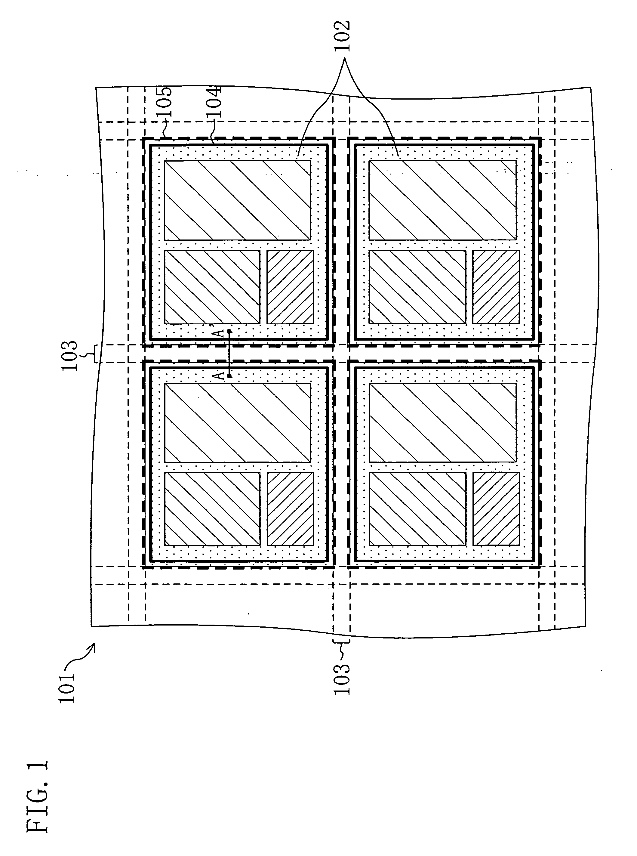
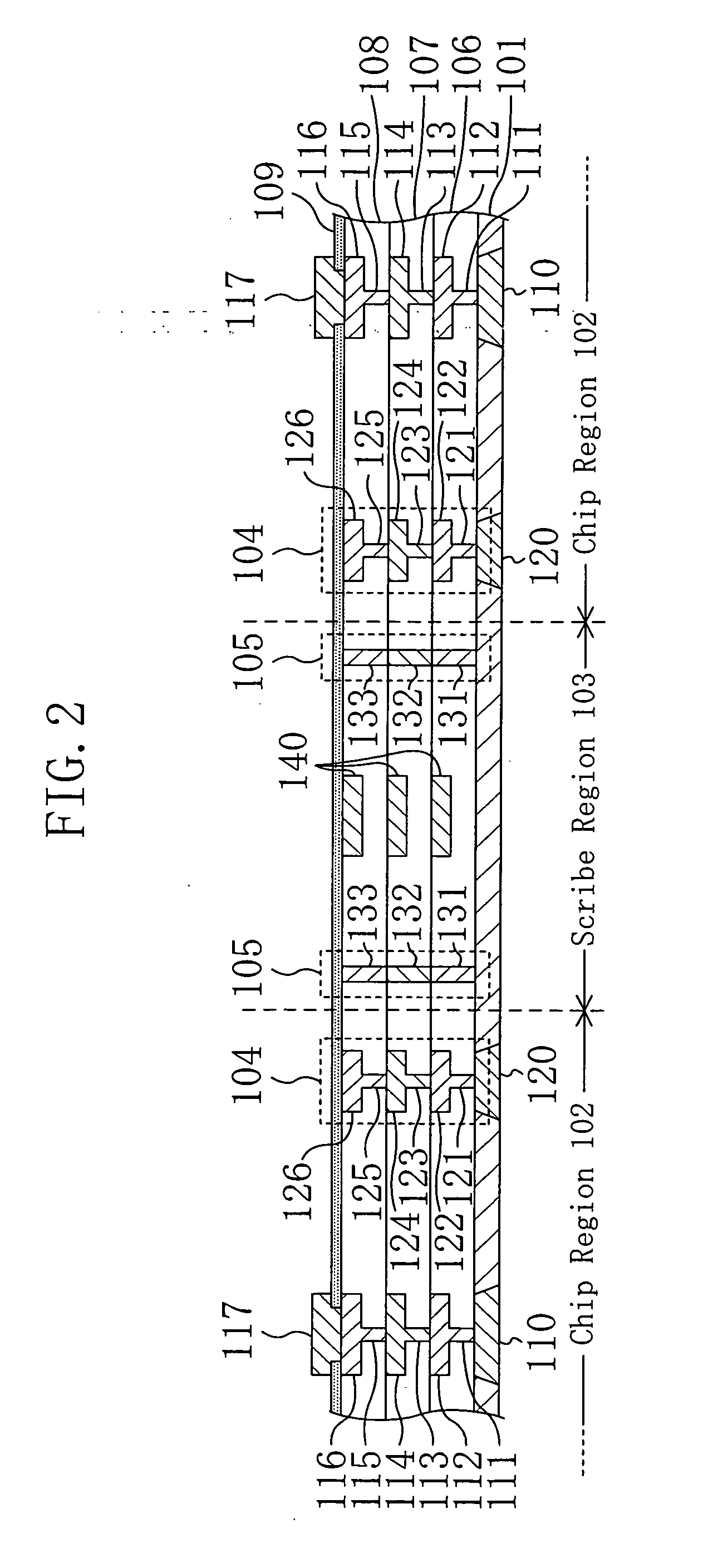
[0068]FIG. 1 is a plan view showing a part of a wafer provided with an electronic device (a semiconductor device having a seal ring singly surrounding a chip region) according to the first embodiment.

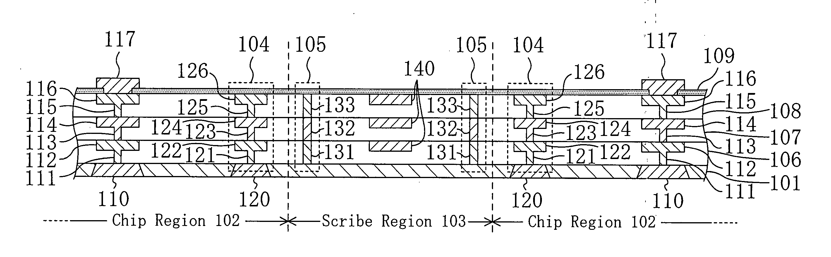
[0069] As shown in FIG. 1, a plurality of chip regions 102, each of which is to serve as a semiconductor device, are arranged in a wafer 101 serving as a semiconductor substrate represented by, e.g., a silicon substrate or the like. Each of the chip regions 102 is provided with an IC (integrated circuit) composed of a plurality of elements and having a specified function. The individual chip regions 102 are defined by scribe regions 103 provided in a grid-like configuration.

[0070] Each one of the semiconductor devices (i.e., each one of the semiconductor chips) is comprised herein of: a chip region 102 in which the...

embodiment 2

[0106] An electronic device according to a second embodiment of the present invention and a method for fabricating the same will be described with reference to the drawings.

[0107]FIG. 16 is a plan view showing a part of a wafer provided with an electronic device (a semiconductor device having a seal ring singly surrounding a chip region) according to the second embodiment.

[0108] As shown in FIG. 16, a plurality of chip regions 202, each of which is to serve as a semiconductor device, are arranged in a wafer 201 serving as a semiconductor substrate represented by, e.g., a silicon substrate or the like. Each of the chip regions 202 is provided with an IC composed of a plurality of elements and having a specified function. The individual chip regions 202 are defined by scribe regions 203 provided in a grid-like configuration.

[0109] Each one of the semiconductor devices (i.e., each one of the semiconductor chips) is comprised herein of: a chip region 202 in which an IC circuit compos...

embodiment 3

[0134] An electronic device according to a third embodiment of the present invention and a method for fabricating the same will be described with reference to the drawings.

[0135]FIG. 23 is a plan view showing a part of a wafer provided with an electronic device (a semiconductor device having a seal ring singly surrounding a chip region) according to the third embodiment.

[0136] As shown in FIG. 23, a plurality of chip regions 302, each of which is to serve as a semiconductor device, are arranged in a wafer 301 serving as a semiconductor substrate represented by, e.g., a silicon substrate or the like. Each of the chip regions 302 is provided with an IC composed of a plurality of elements and having a specified function. The individual chip regions 302 are defined by scribe regions 303 provided in a grid-like configuration.

[0137] Each one of the semiconductor devices (i.e., each one of the semiconductor chips) is comprised herein of: a chip region 302 in which an IC circuit composed...


PUM


Abstract

An electronic device has an element formed in the chip region of a substrate, a plurality of interlayer insulating films formed on the substrate, a wire formed in the interlayer insulating films in the chip region, and a plug formed in the interlayer insulating films in the chip region and connecting to the wire. A seal ring extending through the plurality of interlayer insulating films and continuously surrounding the chip region is formed in the peripheral portion of the chip region. A stress absorbing wall extending through the plurality of interlayer insulating films and discretely surrounding the seal ring is formed outside the seal ring.

Description

CROSS-REFERENCE TO RELATED APPLICATIONS [0001] The teachings of Japanese Patent Application No. 2004-277087, filed Sep. 24, 2004, are entirely incorporated herein by reference, inclusive of the specification, drawings, and claims. BACKGROUND OF THE INVENTION [0002] The present invention relates to an electronic device having a seal ring formed to surround a chip region and a mechanism for protecting the seal ring and to a method for fabricating the same. [0003] An electronic device such as a semiconductor device is typically formed by arranging a large number of IC circuits each composed of a plurality of elements and having a specified function as a matrix on a semiconductor wafer made of, e.g., silicon or the like. [0004] A large number of chip regions arranged in the wafer are separated from each other by scribe regions (scribe lines) provided in a grid-like configuration. After the large number of chip regions are formed in a single wafer through a semiconductor fabrication proc...

Claims


Application Information

Patent Timeline
Patent Type & Authority Applications(United States)
IPC IPC(8): H01L21/30H01L23/544
CPCH01L21/78H01L23/562H01L23/564H01L23/585H01L2224/48091H01L2924/01078H01L2924/3025H01L2924/00014H01L24/48H01L2924/14H01L2224/45147H01L24/45H01L2924/00H01L2224/45015H01L2924/207
Inventor TSUTSUE, MAKOTO
Owner PANNOVA SEMIC
Why Eureka
Try Eureka