Submicron contact fill using a CVD TiN barrier and high temperature PVD aluminum alloy deposition

a technology of cvd tin barrier and submicron contact, which is applied in the direction of semiconductor devices, semiconductor/solid-state device details, electrical apparatus, etc., can solve the problems of not producing consistent filling of contacts, or providing the required electro-migration resistance at the newer submicron contact, etc., to improve the electrical characteristics of contacts, increase the electro-migration resistance, and save costs

Active Publication Date: 2006-04-13
MICROCHIP TECH INC
View PDF8 Cites 7 Cited by
  • Summary
  • Abstract
  • Description
  • Claims
  • Application Information

AI Technical Summary

Benefits of technology

[0008] Forming a contact according to at least one embodiment can provide increased electro-migration resistance, and more consistent and reliable contact fills. More consistent contact fills can, in turn, result in improved electrical characteristics of the contact.
[0009] Various embodiments of the present disclosure provide cost savings and improved cycle time over other more conventional contact formation processes.

Problems solved by technology

This technique, however, does not produce consistently filled contacts, or provide required electro-migration resistance at the newer submicron contact size and circuit element current densities.

Method used


Image

  • Submicron contact fill using a CVD TiN barrier and high temperature PVD aluminum alloy deposition
  • Submicron contact fill using a CVD TiN barrier and high temperature PVD aluminum alloy deposition
  • Submicron contact fill using a CVD TiN barrier and high temperature PVD aluminum alloy deposition

Examples


Embodiment Construction

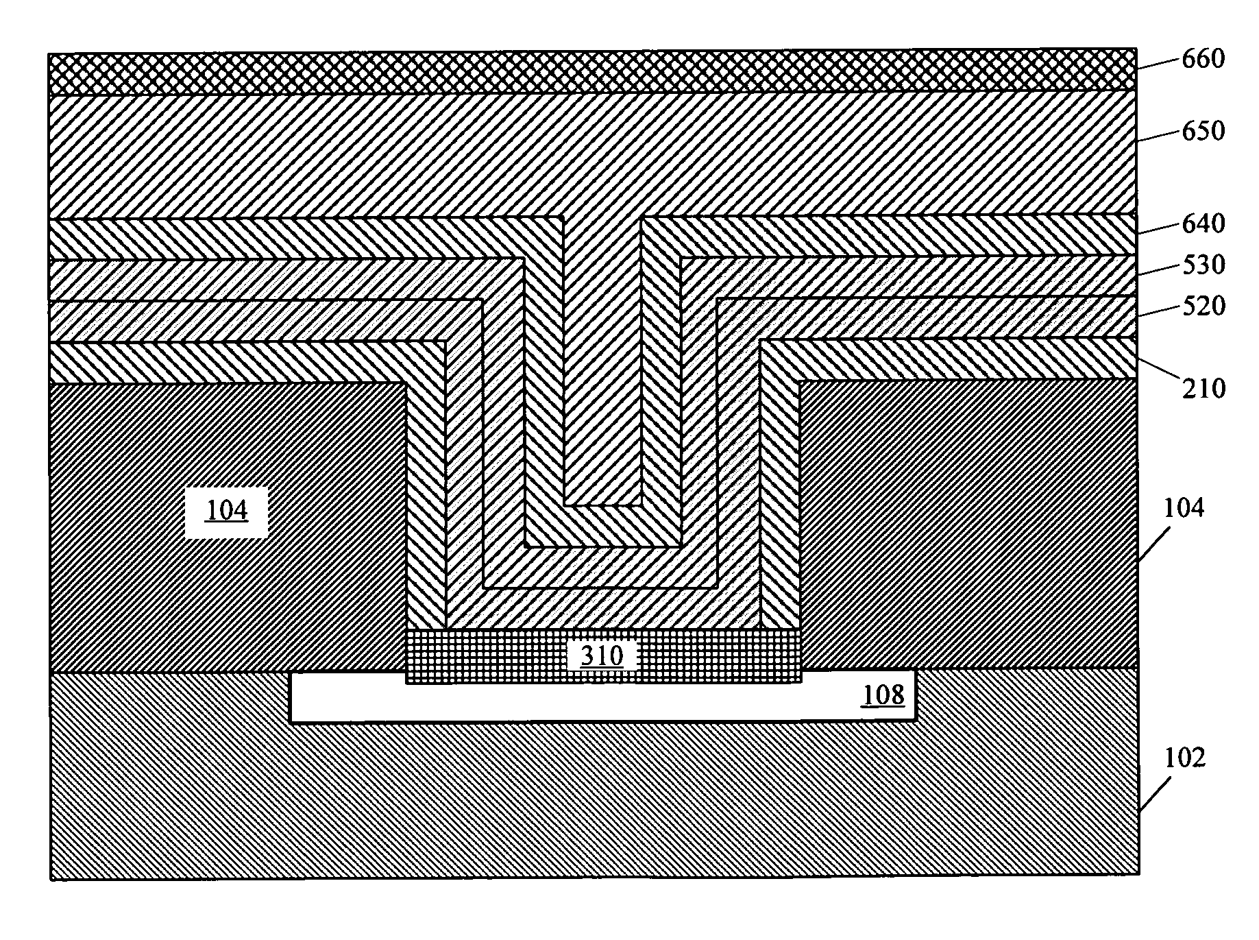
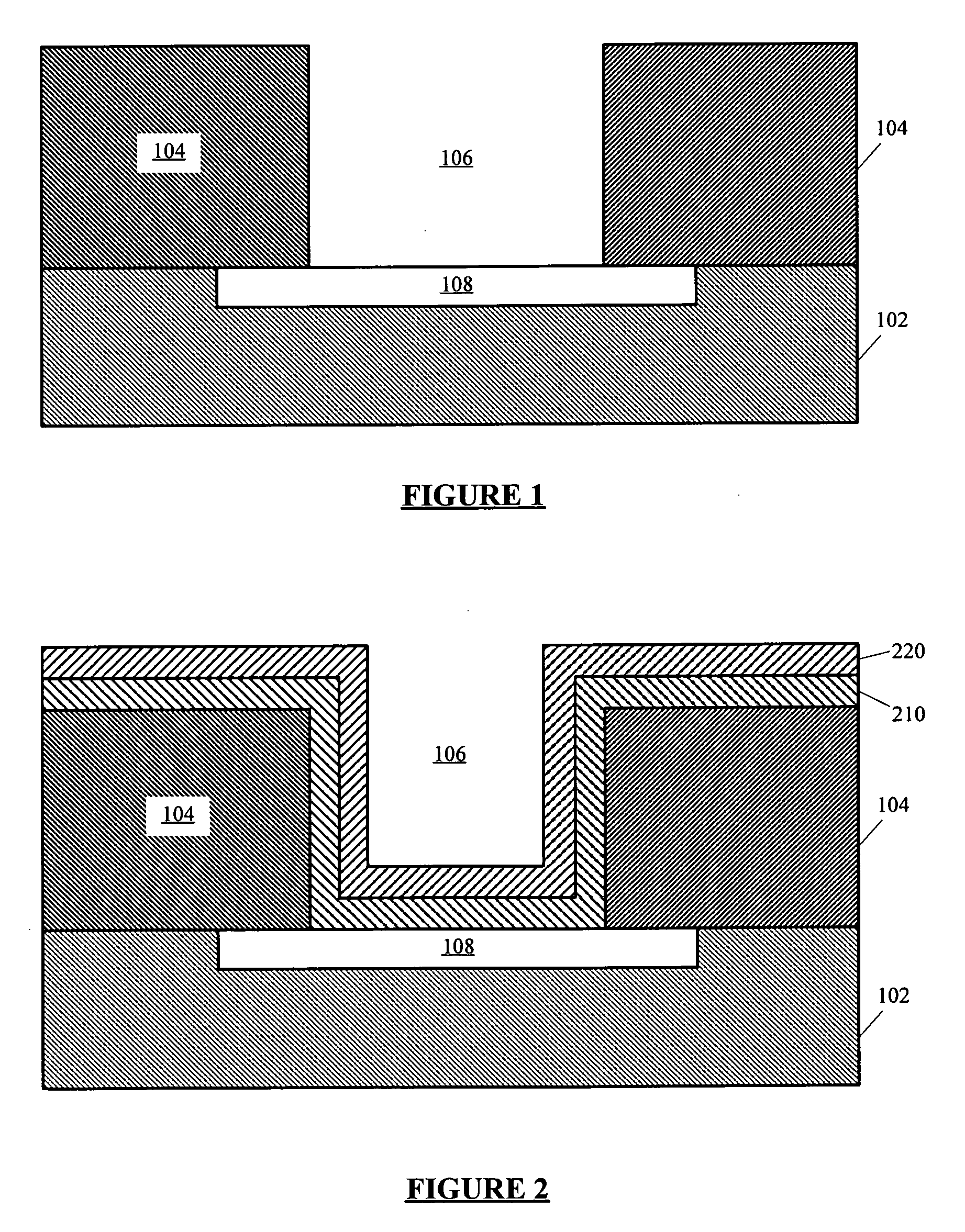
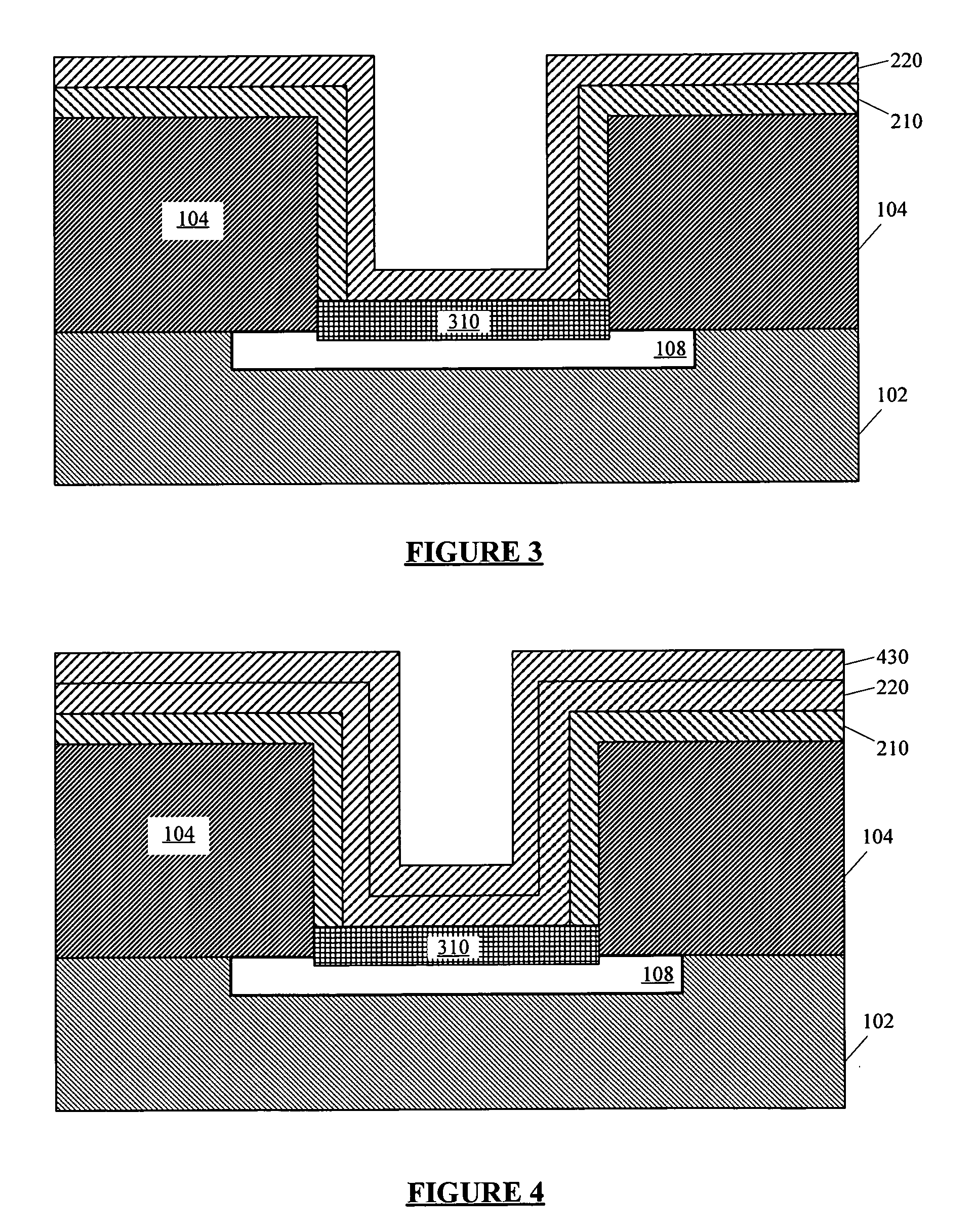
[0015] Referring now to the drawings, the details of specific embodiments of the present invention are schematically illustrated. Like elements in the drawings will be represented by like numbers, and similar elements will be represented by like numbers with a different lower case letter suffix.

[0016] Referring now to FIGS. 1-6, depicted are schematic elevational sections of a portion of a semiconductor integrated circuit illustrating a process of forming a filled contact at various stages of the process, according to a specific embodiment of the present disclosure. FIG. 1 depicts a portion of a semiconductor integrated circuit comprising a plurality of circuit elements, e.g., transistors, formed in a substrate, e.g., silicon, and the circuit elements may be interconnected with circuit conductors (not shown). An insulating film, e.g., an oxide layer 104, is deposited or otherwise formed on the substrate 102. The substrate 102 has circuit elements formed therein (only one element po...


PUM

PropertyMeasurementUnit
temperatureaaaaaaaaaa
thicknessaaaaaaaaaa
thicknessaaaaaaaaaa

Abstract

A submicron contact opening fill using a chemical vapor deposition (CVD) TiN liner/barrier and a high temperature, e.g., greater than about 385° C., physical vapor deposition (PVD) aluminum alloy layer that substantially fills the submicron contact.

Description

RELATED PATENT APPLICATION [0001] This application claims priority to commonly owned U.S. Provisional Patent Application Ser. No. 60 / 614,669; filed Sep. 30, 2004; entitled “Submicron Contact Fill Using a CVD TiN Barrier and High Temperature PVD Aluminum Alloy Deposition,” by Jacob Lee Williams and Harold E. Kline; which is hereby incorporated by reference herein for all purposes.TECHNICAL FIELD OF THE INVENTION [0002] This invention relates generally to semiconductor integrated circuit manufacturing processes, and more particularly to submicron conductive contact filling of holes formed in insulating layers for connection to circuit elements of the semiconductor integrated circuit. BACKGROUND OF THE RELATED TECHNOLOGY [0003] A contact in a semiconductor integrated circuit allows electrical connection between metal conductors and circuit elements, e.g., transistors, in the semiconductor integrated circuit substrate. Generally, an oxide layer is deposited or otherwise formed on the su...

Claims


Application Information

Patent Timeline
Patent Type & Authority Applications(United States)
IPC IPC(8): H01L29/40H01L21/44
CPCH01L21/76846H01L21/7685H01L21/76855H01L21/76856H01L21/76877
Inventor WILLIAMS, JACOB LEEKLINE, HAROLD E.
Owner MICROCHIP TECH INC
Why Eureka
Try Eureka