Optical detector configuration and utilization as feedback control in monolithic integrated optic and electronic arrangements
- Summary
- Abstract
- Description
- Claims
- Application Information
AI Technical Summary
Benefits of technology
Problems solved by technology
Method used
Image

Examples
Embodiment Construction
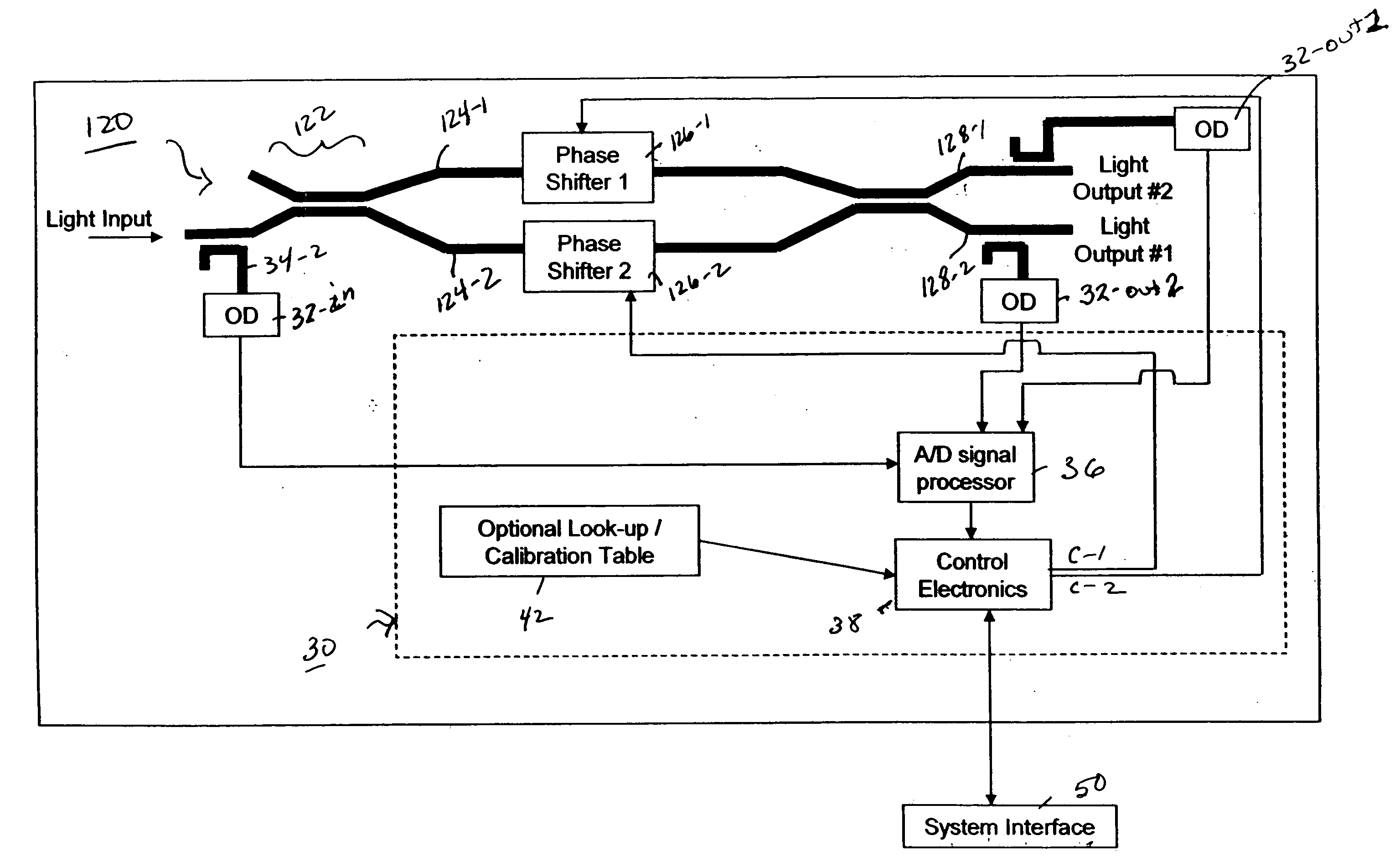
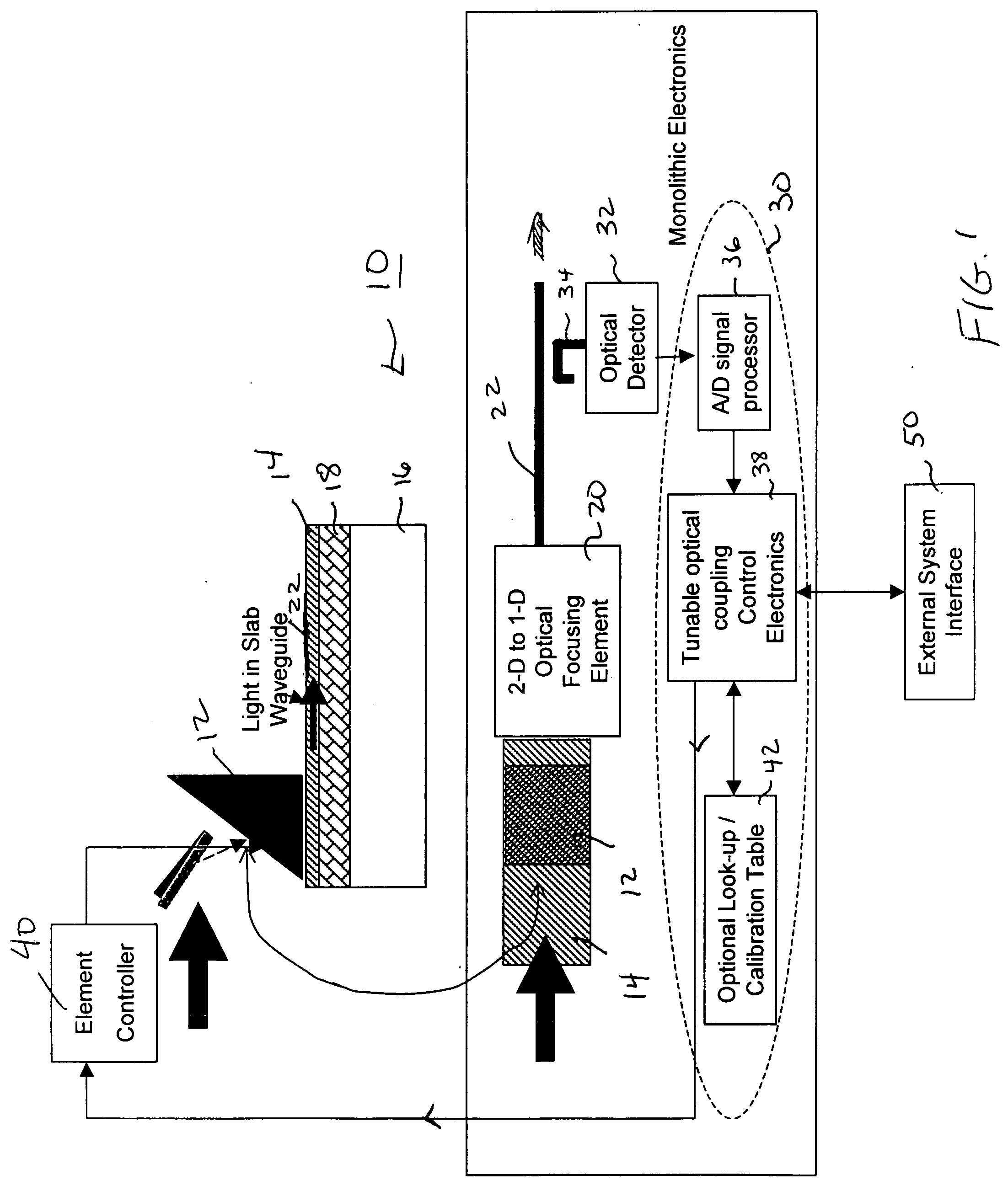
[0021]FIG. 1 illustrates, in a combination of a simplified top view and side view, an exemplary closed-loop feedback-controlled optical input coupling arrangement 10 formed in accordance with the present invention. As described in various other prior references regarding silicon-on-insulator (SOI) optical systems, a silicon prism, such as prism 12, is used to couple an optical signal into a sub-micron thick silicon surface layer 14 of an SOI structure that further comprises a silicon substrate 16 and buried oxide layer 18.
[0022] As shown particularly in to top view of FIG. 1, the coupled optical signal passes through a focusing element 20 and thereafter into a relatively thin optical waveguide 22. Focusing element 20, a silicon-based optical element, is used to convert the two-dimensional propagating optical signal into a one-dimensional optical signal, bounded in both its width and height by waveguide 22. It is well known that the efficiency of this type of coupling arrangement is...
PUM
 Abstract
Description
Claims
Application Information