Electromagnetic wave shielding filter, method of manufacturing the same, PDP apparatus including the same filter

a technology of electromagnetic wave shielding and filter, which is applied in the direction of resistor manufacturing, liquid/solution decomposition chemical coating, incandescent lamp details, etc., can solve the problems of phosphor surface reflection, near-infrared emission, phosphor surface reflection, etc., and achieves high visible light transmittance rays, low electric conductivity, and superior durability

a technology of electromagnetic wave shielding and filter, which is applied in the direction of resistor manufacturing, liquid/solution decomposition chemical coating, incandescent lamp details, etc., can solve the problems of phosphor surface reflection, near-infrared emission, phosphor surface reflection, etc., and achieves high visible light transmittance rays, low electric conductivity, and superior durability

US20060083938A1Inactive Publication Date: 2006-04-20SAMSUNG CORNING PRECISION MATERIALS CO LTD

Image

  • Electromagnetic wave shielding filter, method of manufacturing the same, PDP apparatus including the same filter
  • Electromagnetic wave shielding filter, method of manufacturing the same, PDP apparatus including the same filter
  • Electromagnetic wave shielding filter, method of manufacturing the same, PDP apparatus including the same filter

Examples


experimental example 1

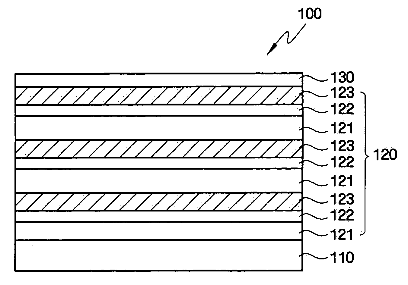
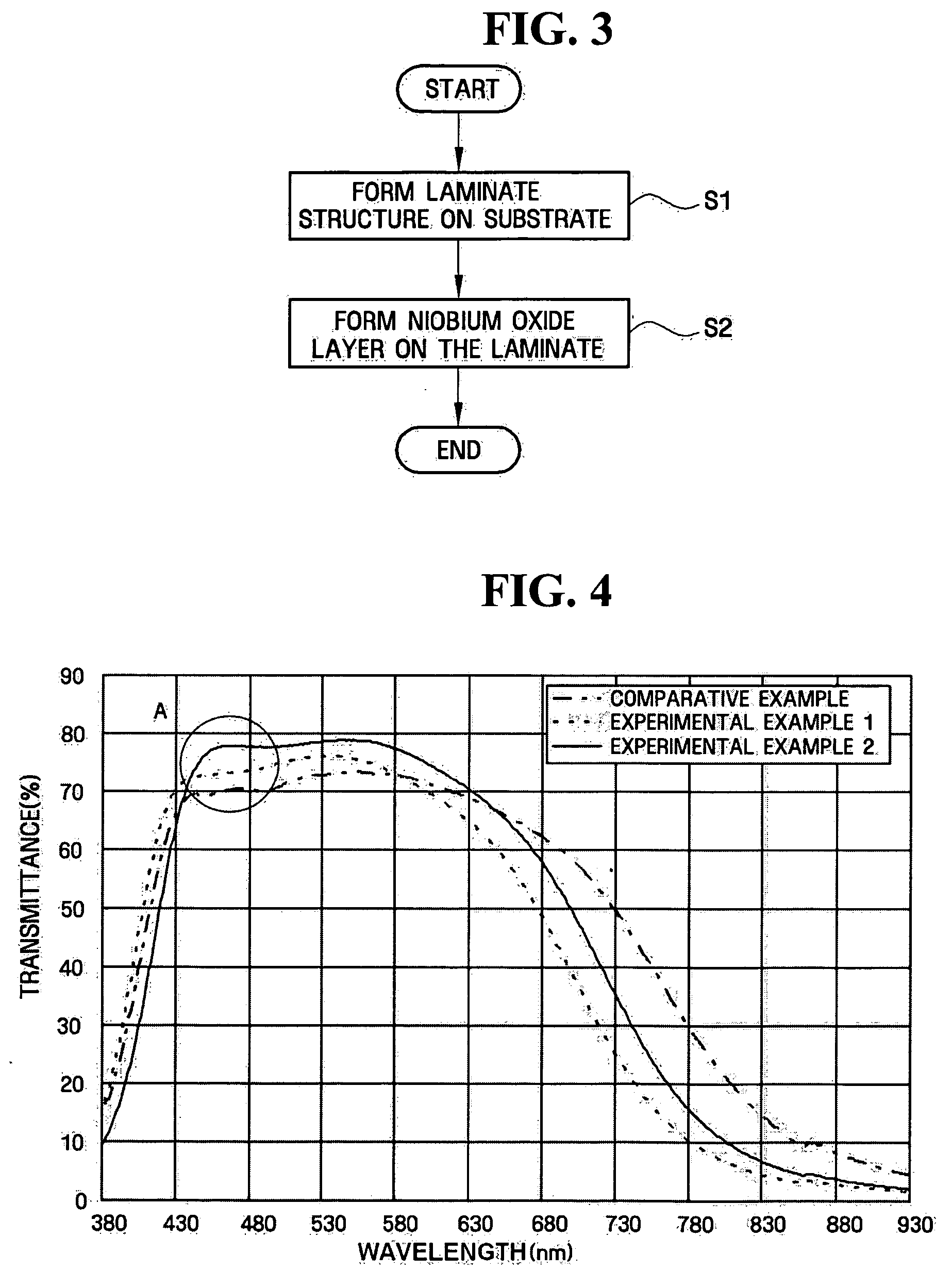
[0077] First, Ar (200 sccm) and O2 (80 sccm) were used as sputtering gases and DC power of 25 kW was applied thereto, forming a 5 nm thick Nb2O5 layer on a substrate, e.g., a transparent glass substrate.

[0078] Next, an AZO layer was formed on the Nb2O5 layer to a thickness of about 5 nm using an aluminum zinc oxide (AZO) target, which contains zinc oxide (ZnO) as a main component and about 1% Al2O3, and Ar (200 sccm) as a sputtering gas, while applying DC power of 1 kW to the target.

[0079] Then, Ar (150 sccm) was used as a sputtering gas and DC power of 1.6 kW power was applied thereto, forming an Ag layer on the AZO layer to a thickness of about 12 nm.

[0080] Next, an ITO target having InO3 containing about 10% SnO2 was used as a target, and Ar (200 sccm) and O2 (80 sccm) were used as sputtering gases, forming an ITO layer to a thickness of about 5 nm on the Ag layer.

[0081] Subsequently, a 56 nm thick Nb2O5 layer, a 5 nm thick AZO layer, a 14 nm thick Ag layer, and a 5 nm thick ...

experimental example 2

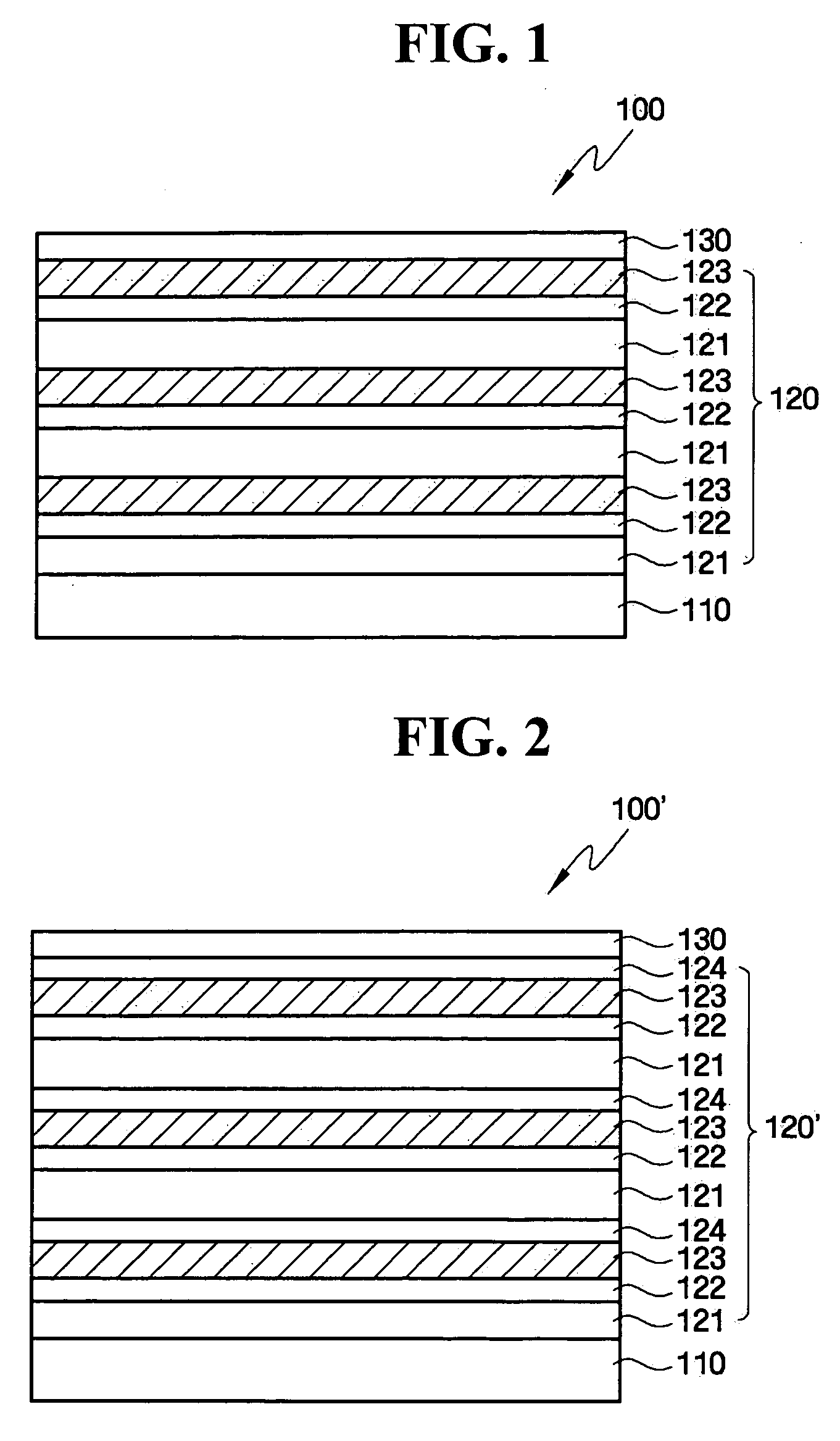
[0082] An electromagnetic wave shielding filter was manufactured in the same manner as in Experimental Example 1 except that a protective layer formed on an Ag layer was comprised of AZO. That is, the structure of the electromagnetic wave shielding filter prepared in this example was as follows: Substrate / Nb2O5 layer / AZO layer / Ag layer / AZO layer / Nb2O5 layer / AZO layer / Ag layer / AZO layer / Nb2O5 layer / AZO layer / Ag layer / AZO layer / Nb2O5 layer / .


PUM

PropertyMeasurementUnit
thicknessaaaaaaaaaa
thicknessaaaaaaaaaa
thicknessaaaaaaaaaa

Abstract

An electromagnetic wave shielding filter that has low electric conductivity, high visible light transmittance and good durability, a method of manufacturing the electromagnetic wave shielding filter, and a PDP apparatus including the electromagnetic wave shielding filter. The electromagnetic wave shielding filter includes a laminate structure including multiple stacks each consisting of a niobium oxide layer, a first protective layer having a ZnO as a main component, and a metal layer sequentially laminated in that order, the multiple stacks formed by repeatedly laminating the respective layers at least three times, and a niobium oxide layer formed on the laminate structure.

Description

[0001] This application claims priority from Korean Patent Application No. 10-2004-0083184 filed on Oct. 18, 2004, in the Korean Intellectual Property Office, the disclosure of which is incorporated herein in its entirety by reference. BACKGROUND OF THE INVENTION [0002] 1. Field of the Invention [0003] The present invention relates to an electromagnetic wave shielding filter, a method of manufacturing the same and a plasma display panel (“PDP”) apparatus including the same. More particularly, the present invention relates to an electromagnetic wave shielding filter which has low electric conductivity, high visible light transmittance and good durability, a method of manufacturing the same and a PDP apparatus including the same. [0004] 2. Description of the Related Art [0005] As modem society becomes more information-oriented, photoelectronic devices and apparatuses are advancing and are becoming more widespread. In particular, image display devices are being widely used in a variety...

Claims


Application Information

Patent Timeline
20 Apr 2006
Publication
US20060083938A1
IPC
B32B15/04; B32B9/00; B32B19/00; B05D5/12; G09F9/00; H05K9/00
CPC
H01J11/12; H01J11/44; H01J2211/446; H05K9/0096
Inventors
KIM, EUI-SOO; WOO, KYEONG-KEUN