Model-based pattern characterization to generate rules for rule-model-based hybrid optical proximity correction

a hybrid optical proximity and model-based technology, applied in the field of system and method for providing optical proximity correction, can solve the problems of ic design and semiconductor fabrication process, ic can be more complex, and the final semiconductor product yield is lower

Active Publication Date: 2006-04-20
APPLIED MATERIALS INC
View PDF3 Cites 82 Cited by
  • Summary
  • Abstract
  • Description
  • Claims
  • Application Information

AI Technical Summary

Benefits of technology

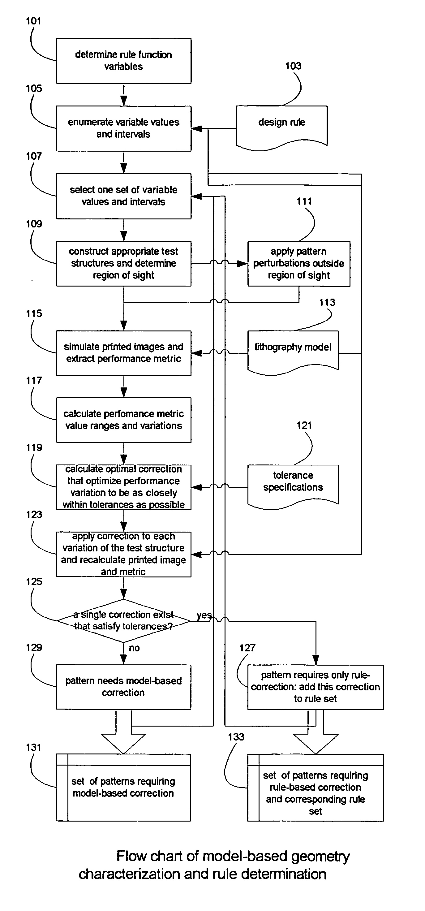
[0015] In accordance with the present invention, a system and method are provided to enumerate and analyze a series of layout patterns conforming to a set of design rules through simulation using a lithography model, typically calibrated to empirical data, which would be used in the model-based OPC of integrated circuit (IC) layouts. Such analysis results in a set of selection rules that can be applied to an IC layout to identify portions of the IC layout that can be corrected by rule-based OPC that would otherwise be corrected by model-based OPC, and portions of the IC layout that need to be corrected by model-based OPC. The system and method of the present invention preferably determine whether a correction rule can be found for each pattern according to prespecified performance metrics under different variations of the pattern. Those patterns for which correction rules can be found are deemed suitable for rule-based OPC. Those patterns for which correction rules cannot be found are considered to require model-based OPC. The method and system can optionally generate correction rules together with the selection rules. Additionally, a system and method for OPC of a physical layout are provided that use the generated rules to select layout portions that are rule-correctable, and apply the corresponding correction rules, and correct the remaining layout using model-based OPC, which takes into account the rule-based corrections.

Problems solved by technology

Moreover, smaller geometries allow silicon chips to contain more circuit elements, and, hence, the integrated circuit (IC) can be more complex, and more copies of the same die can be produced on a single silicon wafer.
Consequently, IC designs and semiconductor fabrication processes are extremely complex, since hundreds of processing steps may be involved.
Occurrence of a mistake or small error at any of the design or process steps may necessitate redesign or cause lower yield in the final semiconductor product, where yield may be defined as the number of functional devices produced by the process as compared to the theoretical number of devices that could be produced assuming no bad devices.
Improving time-to-market and yield is a critical problem in the semiconductor manufacturing industry and has a direct economic impact on the semiconductor industry.
With ever decreasing feature sizes, increasing pattern densities, and difficulty experienced in the advancement of IC manufacturing equipment, manufacturing of modem IC designs has encountered substantial impediments and concomitant yield problems within the near- and sub-wavelength regime, where the feature dimension is at or below the wavelength of the light source.
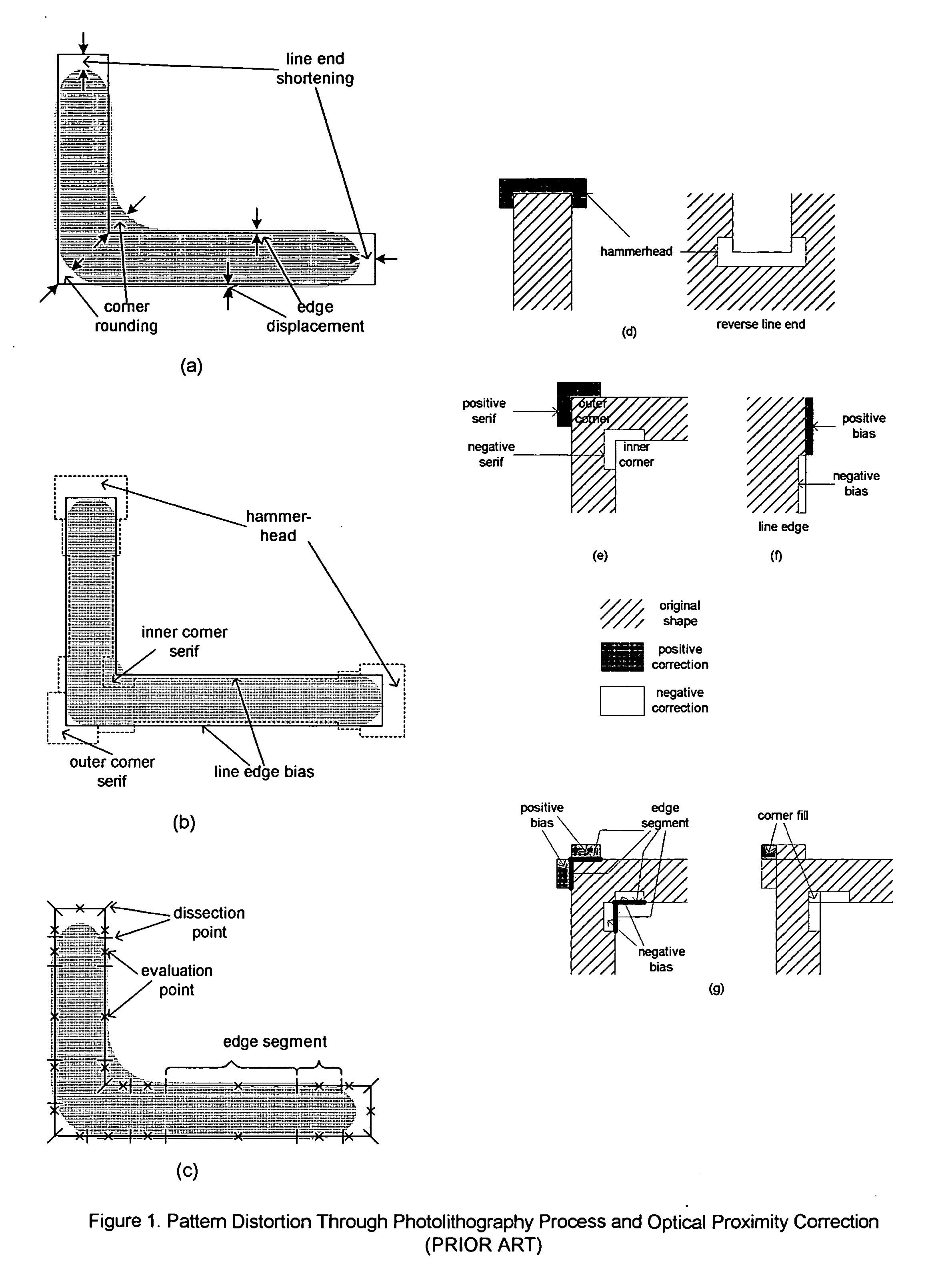
With the emergence of near- and sub-wavelength lithography, patterns projected to the wafer through the lithography process are severely distorted.
However, rule-based OPC is not very accurate, and, hence, is used only for 0.25 μm or larger technology nodes or on non-critical layers of more advanced technology nodes (0.18 μm or smaller), such as metal, or layers that contain only relatively large geometries whose accuracy requirements are more relaxed.
Moreover, generation of correction rules is non-systematic and often requires experience, and as the complexity of the geometries increases, the number of rules and possibly complexity of the rules increase as well, which makes them difficult to maintain.
On the other hand, due to finer granularity of the correction, the resulting corrected layout by a model-based approach is typically more complex than that by a rule-based approach.
However, determination of the selection rules, like the determination of the correction rules, is still very much a manual process, and is usually a time-consuming and ad hoc process.
Moreover, the accuracy performance of these rules is difficult to quantify a priori.
Hence, it is difficult to predict the accuracy of the correction results when they are applied.

Method used


Image

  • Model-based pattern characterization to generate rules for rule-model-based hybrid optical proximity correction
  • Model-based pattern characterization to generate rules for rule-model-based hybrid optical proximity correction
  • Model-based pattern characterization to generate rules for rule-model-based hybrid optical proximity correction

Examples


Embodiment Construction

[0026] The present invention is particularly applicable to a computer-implemented software-based IC design system for performing lithography-model-based pattern characterization and rule generation, and producing an IC design by applying hybrid optical proximity correction (OPC) using the generated rules for correcting an IC design layout, and it is in this context that the various embodiments of the present invention will be described. It will be appreciated, however, that the IC design system and method for providing hybrid OPC in accordance with the various embodiments of the present invention have greater utility, since they may be implemented in hardware or may incorporate other modules or functionality not described herein.

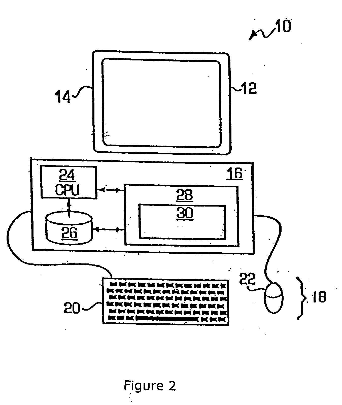
[0027]FIG. 2 is a block diagram illustrating an example of an IC design system 10 for providing lithography-model-based pattern characterization and rule generation, and hybrid OPC in accordance with one embodiment of the present invention implemented on a ...


PUM


Abstract

A system and method are provided for analyzing layout patterns via simulation using a lithography model to characterize the patterns and generate rules to be used in rule-based optical proximity correction (OPC). The system and method analyze a series of layout patterns conforming to a set of design rules by simulation using a lithography model to obtain a partition of the pattern spaces into one portion that requires only rule-based OPC and another portion that requires model-based OPC. A corresponding hybrid OPC system and method are also introduced that utilize the generated rules to correct an integrated circuit (IC) design layout which reduces the OPC output complexity and improves turnaround time.

Description

CROSS-REFERENCE TO RELATED APPLICATION [0001] This application relates to U.S. Provisional Patent Application No. 60 / 619,208 filed on Oct. 15, 2004 entitled METHOD FOR MODEL BASED GEOMETRICAL CHARACTERIZATION TO GENERATE RULES FOR RULE-MODEL BASED HYBRID OPTICAL PROXIMITY CORRECTION.BACKGROUND OF THE INVENTION [0002] 1. Field of the Invention [0003] The present invention relates generally to a system and method for designing integrated circuits or migrating integrated circuit designs from one technology node to another for fabrication by a semiconductor manufacturing process and, more particularly, to a system and method for providing optical proximity correction for integrated circuit design layouts. [0004] 2. Description of the Prior Art [0005] The semiconductor manufacturing industry is continually evolving semiconductor device designs and fabrication processes and developing new processes to produce smaller and smaller geometries of the designs being manufactured. Semiconductor ...

Claims


Application Information

Patent Timeline
Patent Type & Authority Applications(United States)
IPC IPC(8): G06F17/50
CPCG03F1/144G03F1/36G03F7/70441G03F7/705
Inventor ZHANG, YOUPING
Owner APPLIED MATERIALS INC
Why Eureka
Try Eureka