Nanoscale latches and impedance-encoded logic for use in nanoscale state machines, nanoscale pipelines, and in other nanoscale electronic circuits

a technology of impedance-encoded logic and latches, applied in the field of nanoscale latches, can solve the problems of signal degradation to make such cascaded logic circuits unusable, the implementation of sequential diode resistor logic is difficult, and the inherently degraded signals of diode resistor logi

Active Publication Date: 2006-04-27
HEWLETT-PACKARD ENTERPRISE DEV LP
View PDF12 Cites 6 Cited by
  • Summary
  • Abstract
  • Description
  • Claims
  • Application Information

AI Technical Summary

Benefits of technology

[0008] Various embodiments of the present invention are directed to implementation and use of logic-state-storing, impedance-encoded nanoscale latches that store logic values as impedance states within nanoscale electronic circuits that employ impedance-driven logic. In certain of these embodiments, use of nanoscale latches together with nanoscale electronic circuits that employ impedance-driven logic avoids cumulative degradation of voltage margins along a cascaded series of logic circuits and provides for temporary storage of intermediate logic values, allowing for practical interconnection of nanowire-crossbar-implemented logic circuits through nanoscale latches to other nanowire-crossbar-implemented logic circuits in order to implement complex, nanoscale-logic-circuit pipelines, nanoscale-logic-circuit-based state machines, and other complex logic devices with various different interconnection topologies and corresponding functionalities.

Problems solved by technology

Diode-resistor logic inherently degrades signals because of voltage drops across diodes and pullup and pulldown resistors.
Cascading diode logic produces cumulative signal degradation that, when diode logic is cascaded to any significant depth, produces sufficient signal degradation to make such cascaded logic circuits unusable.
Diode-resistor logic also lacks the ability to store logic states, so that implementation of sequential diode-resistor logic is difficult.

Method used


Image

  • Nanoscale latches and impedance-encoded logic for use in nanoscale state machines, nanoscale pipelines, and in other nanoscale electronic circuits
  • Nanoscale latches and impedance-encoded logic for use in nanoscale state machines, nanoscale pipelines, and in other nanoscale electronic circuits
  • Nanoscale latches and impedance-encoded logic for use in nanoscale state machines, nanoscale pipelines, and in other nanoscale electronic circuits

Examples


Embodiment Construction

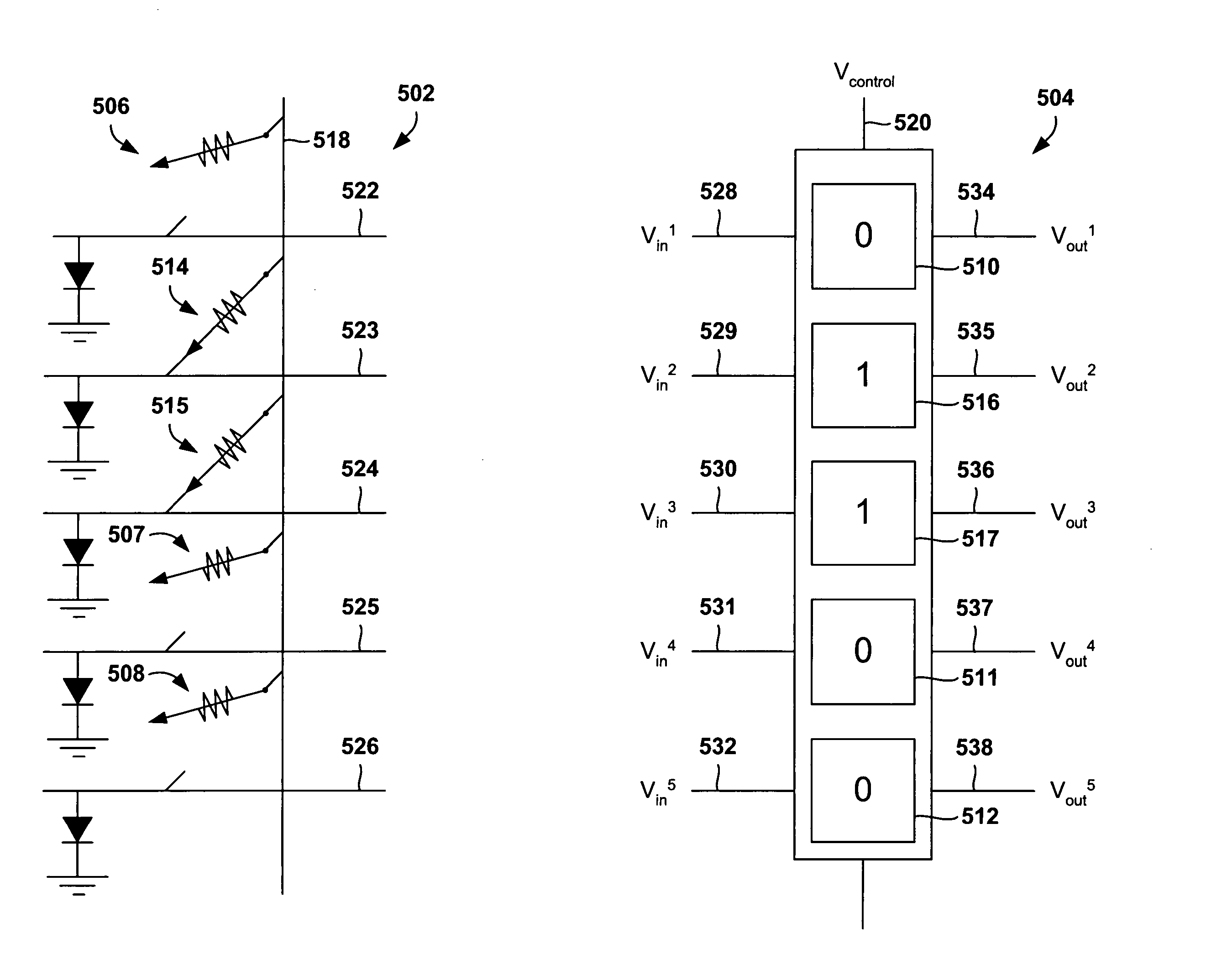
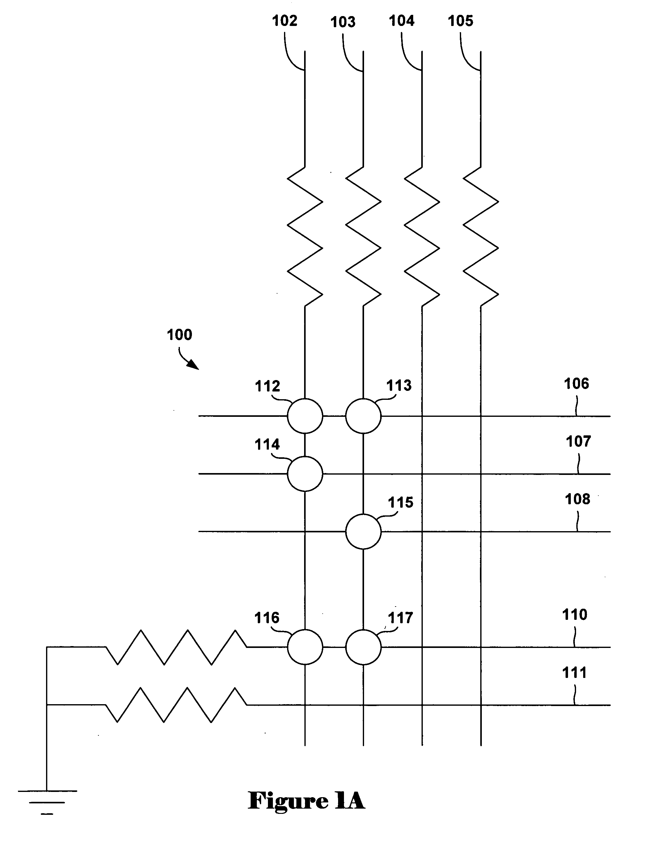
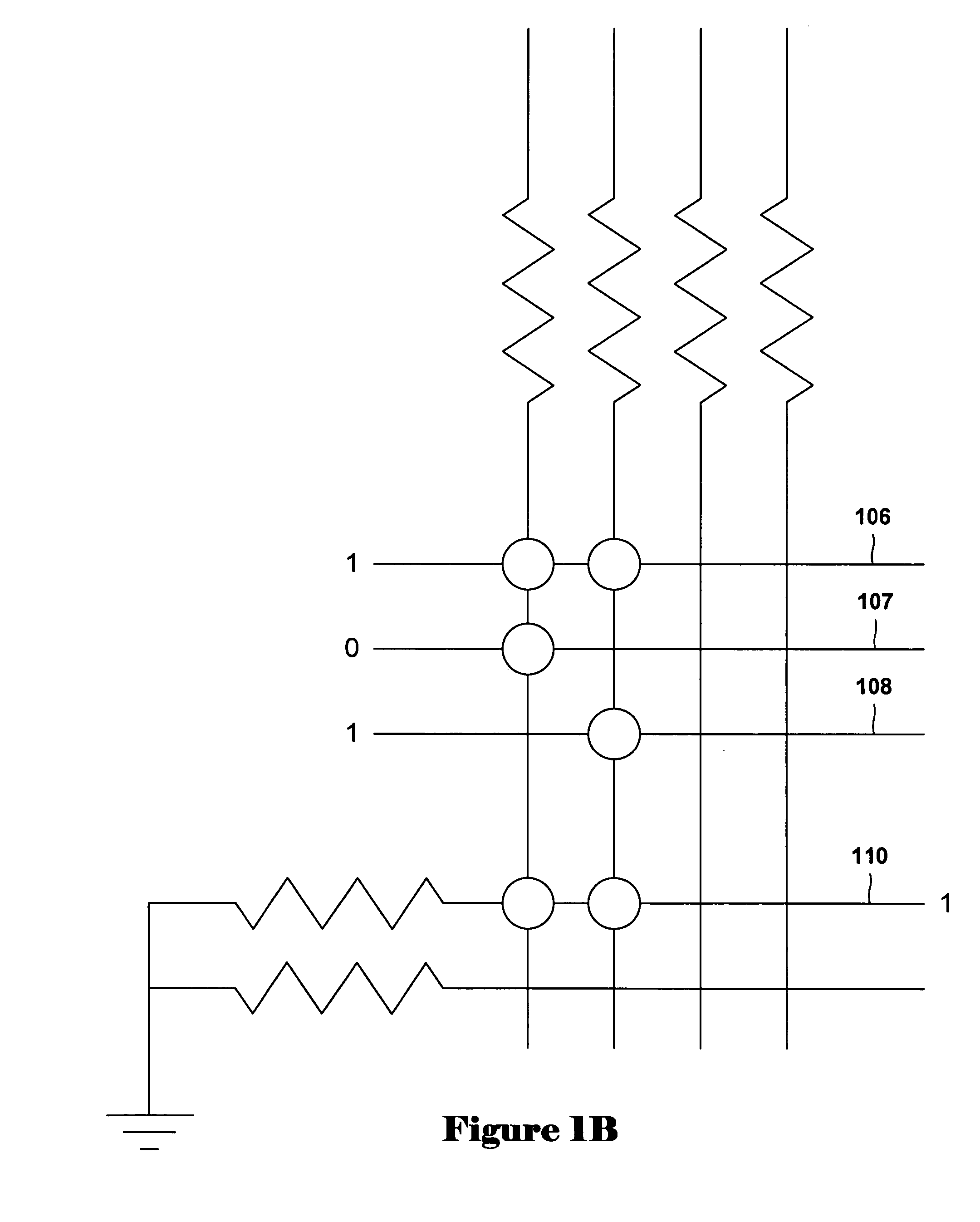
[0022] Various embodiments of the present invention are directed to constructing and using nanoscale impedance-encoded latches (“NIELs”) for storing logic states produced and consumed by nanoscale impedance-driven logic circuits (“NIDLCs”). NIELs enable NIDLCs to be cascaded to create more complex logic functions than are possible in a single stage of logic. Signals degraded in passing through impedance-driven logic stages can be boosted, or restored, through operation of one or more intervening NIELs. The NIDLCs and intervening NIELs can be clocked to produce pipelines, state machines, and more complex logic circuits. The following discussion provides general information and both an overview and details of the present invention in a number of subsections, including: (1) hysteretic resistors; (2) NIELs; (3) latch arrays; (4) diode-resistor logic; (5) impedance-driven logic; (6) an impedance-encoded and impedance-driven logic stage; (7) pipelines; (8) pipeline operation; (9) state ma...


PUM


Abstract

Various embodiments of the present invention are directed to implementation and use of logic-state-storing, impedance-encoded nanoscale, impedance-encoded latches that store logic values as impedance states within nanoscale electronic circuits that employ impedance-driven logic. In certain of these embodiments, use of nanoscale, impedance-encoded latches together with nanoscale electronic circuits that employ impedance-driven logic avoids cumulative degradation of voltage margins along a cascaded series of logic circuits and provides for temporary storage of intermediate logic values, allowing for practical interconnection of nanowire-crossbar-implemented logic circuits through nanoscale, impedance-encoded latches to other nanowire-crossbar-implemented logic circuits in order to implement complex, nanoscale-logic-circuit pipelines, nanoscale-logic-circuit-based state machines, and other complex logic devices with various different interconnection topologies and corresponding functionalities.

Description

TECHNICAL FIELD [0001] The present invention is related to nanoscale electronics and, in particular, to nanoscale latches and methods for using impedance-encoded nanoscale latches in impedance-driven, nanoscale logic. BACKGROUND OF THE INVENTION [0002] Years of research and development efforts have led to significant achievements in the nanoscale electronics field. Nanoscale electronics generally refer to electronic circuits, fabricated by any of various methods, which include signal lines with widths less than 100 nm and active and passive electronic components, each fabricated from one to tens or hundreds of molecules. In one promising nanoscale electronic circuit architecture, nanowire crossbars are fabricated from a first set of closely spaced, parallel nanowires overlaid by a second set of closely spaced, parallel nanowires, with electronic components, such as diodes, resistors, and passive connections fabricated within the overlap regions, or nanowire junctions, where nanowire...

Claims


Application Information

Patent Timeline
Patent Type & Authority Applications(United States)
IPC IPC(8): H03K19/00
CPCB82Y10/00G11C13/02G11C2213/77G11C2213/81H03K19/02Y10S977/789H03K19/177
Inventor SNIDER, GREGORY S.KUEKES, PHILIP J.
Owner HEWLETT-PACKARD ENTERPRISE DEV LP
Why Eureka
Try Eureka