Laser ablation method

Inactive Publication Date: 2006-04-27
INTEL CORP
View PDF7 Cites 148 Cited by
  • Summary
  • Abstract
  • Description
  • Claims
  • Application Information

AI Technical Summary

Problems solved by technology

Heating can cause problems with microcracking, delamination, and particles, all of which can impact semiconductor die yields and reliability.
Laser scribing/dicing through multiple layers can compound thermal effects problems.
In either case, microcracking, delamination, and particles can result.
The interaction between the laser pulse and the plasma plume can also create pr

Method used


Image

  • Laser ablation method
  • Laser ablation method
  • Laser ablation method

Examples


Embodiment Construction

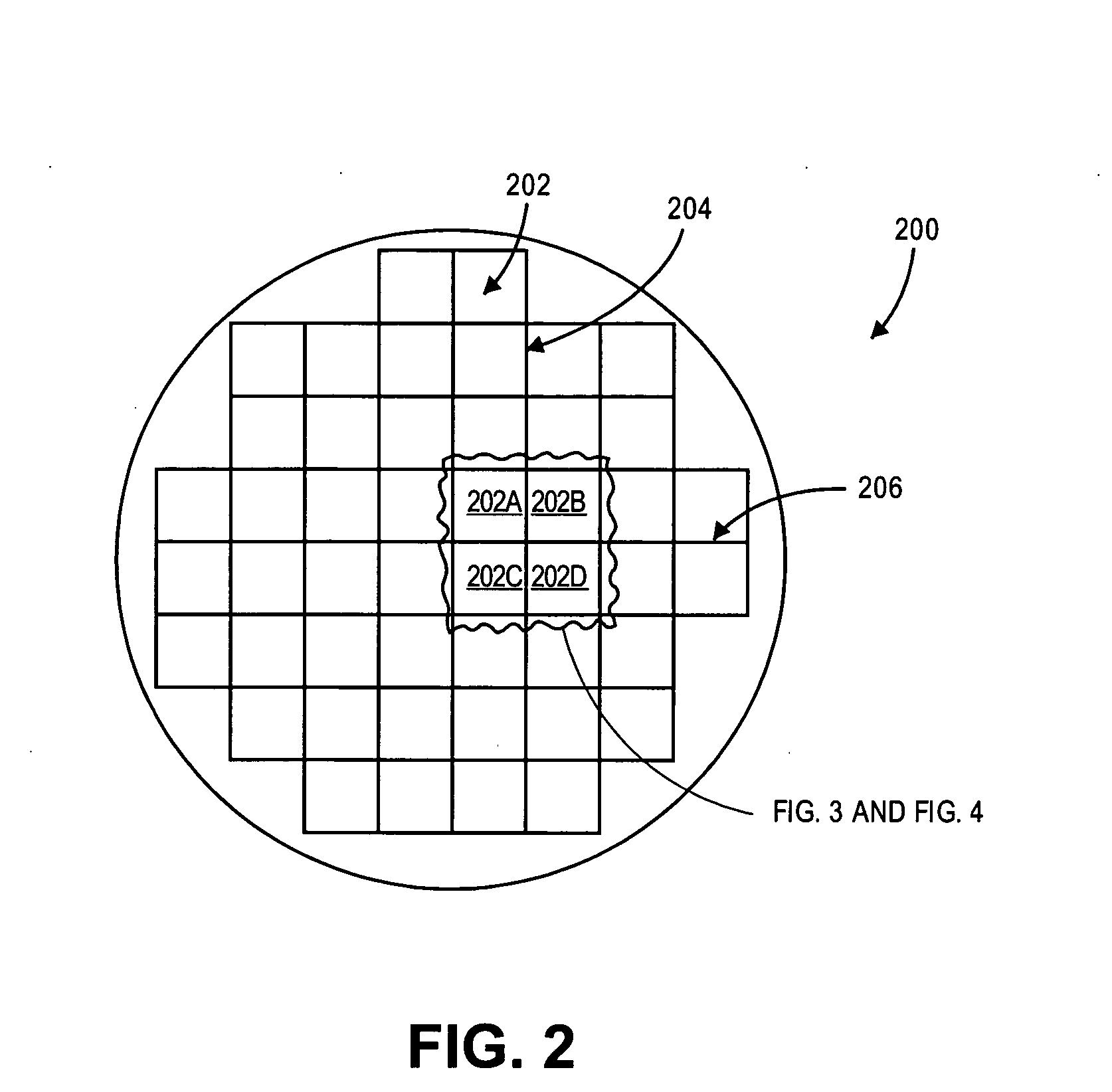
[0014] In the following detailed description, a method for laser scribing / dicing semiconductor substrates is disclosed. Reference is made to the accompanying drawings within which are shown, by way of illustration, specific embodiments by which the present invention may be practiced. In other instances, well known features may be omitted or simplified in order not to obscure embodiments of the present invention. It is to be understood that other embodiments may exist and that other structural changes may be made without departing from the scope and spirit of the present invention.

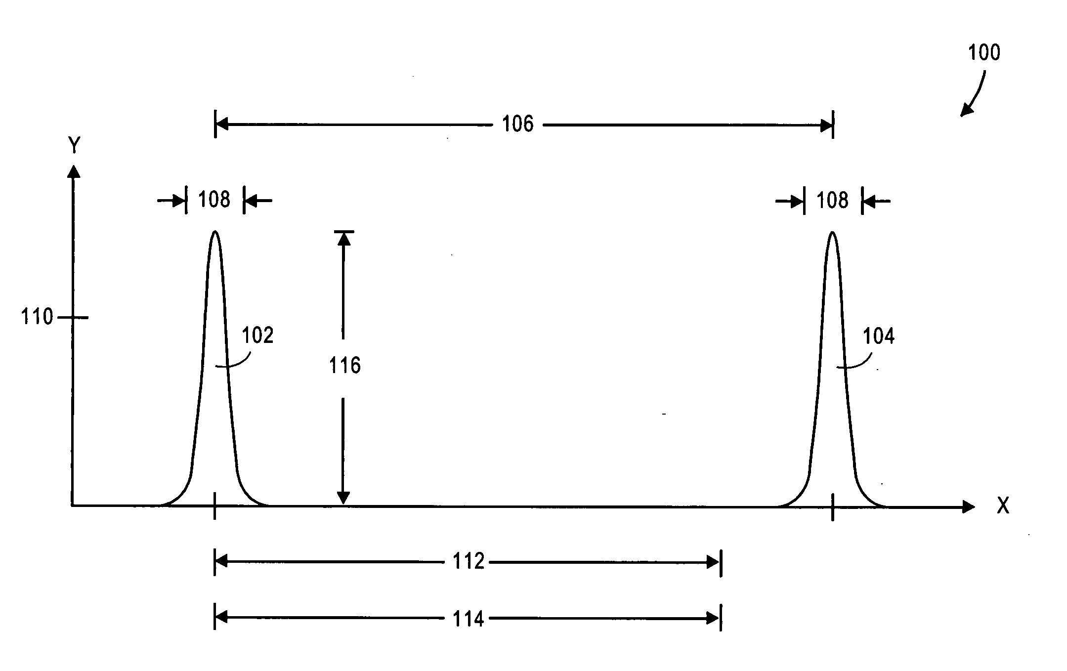
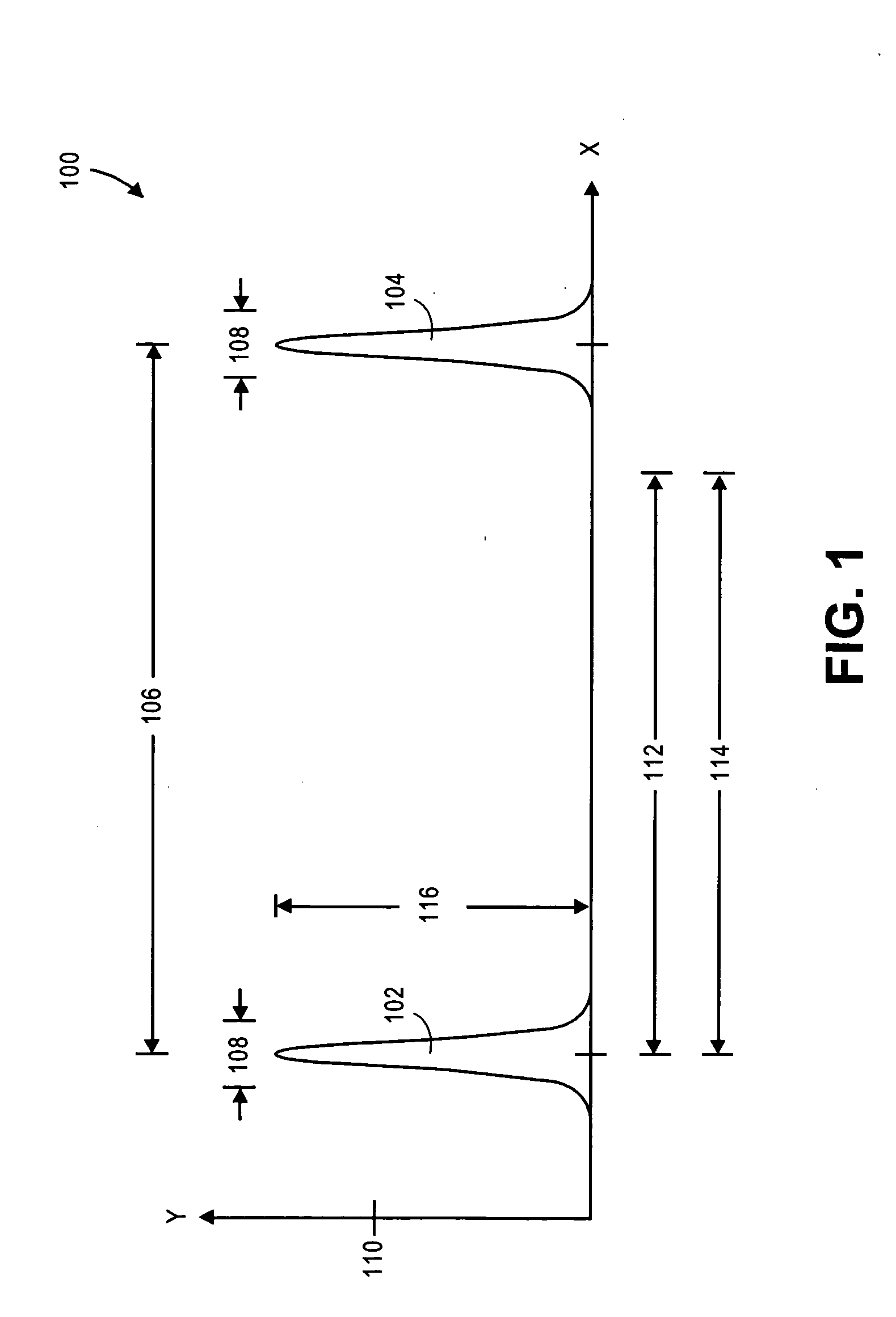
[0015] In accordance with an embodiment of the present invention, specific laser pulse durations and repetition rates are incorporated into a laser scribing / dicing process. The disclosed processes can reduce / eliminate factors that contribute to thermal effects, explosive melting and evaporation, and laser / plasma interactions, thereby reducing microcracking, delamination, and particles that can affect semic...


PUM

PropertyMeasurementUnit
Timeaaaaaaaaaa
Timeaaaaaaaaaa
Timeaaaaaaaaaa

Abstract

A combination of specific laser pulse durations and repetition rates are incorporated into a semiconductor wafer laser scribing/dicing process. The disclosed combination can reduce factors that contribute to thermal effects, explosive melting and evaporation, and laser/plasma interactions, thereby reducing problems with microcracks, delamination, and particles that can affect semiconductor die yields and reliability.

Description

FIELD OF THE INVENTION [0001] Embodiments of the present invention relate generally to laser micromachining and more specifically to the laser micromachining of semiconductor substrates. BACKGROUND OF THE INVENTION [0002] The heat generated during the scribing / dicing of semiconductor wafers can be a concern when using conventional (nanosecond) lasers. Heating can cause problems with microcracking, delamination, and particles, all of which can impact semiconductor die yields and reliability. Heat is generated when optical power from the laser pulse is coupled to the lattice degrees of freedom of the material being lased. When this occurs, high energy electrons (excited by photons from the laser) transfer energy to phonons through electron-phonon interactions. This typically occurs within a matter of tens of picoseconds. As a result, the material heats, melts, and then upon reaching its photo ablation threshold, evaporates. [0003] Due to the thermal nature of nanosecond pulsed laser a...

Claims


Application Information

Patent Timeline
IPC IPC(8): H01L21/78B23K26/38
CPCB23K26/0635B23K26/38B23K2201/40H01L21/78B23K26/0624B23K2101/40
Inventor LI, ERIC J.RUMER, CHRISTOPHER L.STRELTSOV, ALEXANDER M.BLOCKER, MARK A.VORONOV, SERGEI L.
Owner INTEL CORP
Why Eureka
Try Eureka