Laser micromachining method

a laser scribing and micromachining technology, applied in the field of micromachining, can solve the problems of wafer surface, laser scribing, wafer cutting, etc., and achieve the effect of solving the problem of a number of challenges

Inactive Publication Date: 2007-01-30
INTEL CORP
View PDF3 Cites 46 Cited by
  • Summary
  • Abstract
  • Description
  • Claims
  • Application Information

AI Technical Summary

Problems solved by technology

However, sawing may not be suitable for cutting through advanced-materials formed on the wafer surface (i.e., low-k dielectrics).
Laser scribing, however, is confronted with a number of challenges.
Differences in ablation thresholds of materials formed on the wafer can complicate the laser ablation process.
So, while conventional lasers may be capable of ablating silicon and silicon carbide, ablation of silicon nitride and silicon dioxide is more difficult.
Underlying layer ablation can proceed explosively and thereby produce thermal and mechanical stress, damage, peeling, and cracking in the film stack, as well as generate surface particles.
However, there are a number of limitations associated with these systems.
Shorter wavelength (266 nm) Nd:YAG lasers (4.7 eV photon energy) are limited by their low output power.
Higher power ultraviolet (UV) lasers, such as excimer lasers (e.g., Krypton Fluoride (KrF) lasers (248 nm or 5.0 eV photon energy) and Fluorine (F2) lasers (157 nm or 7.9 eV photon energy) are limited by their low repetition rates, limited power output, and reliability.
In addition, complex and costly UV optical components are needed to project and focus the shorter wavelength laser beams onto the workpiece in order to achieve the power densities needed for ablation.
However, while the overall laser scribing quality of ultrafast lasers may be superior to that of conventional lasers, they are limited by their low processing throughputs and the difficulties related to their stability, maintenance, and cost.

Method used


Image

  • Laser micromachining method
  • Laser micromachining method
  • Laser micromachining method

Examples


Embodiment Construction

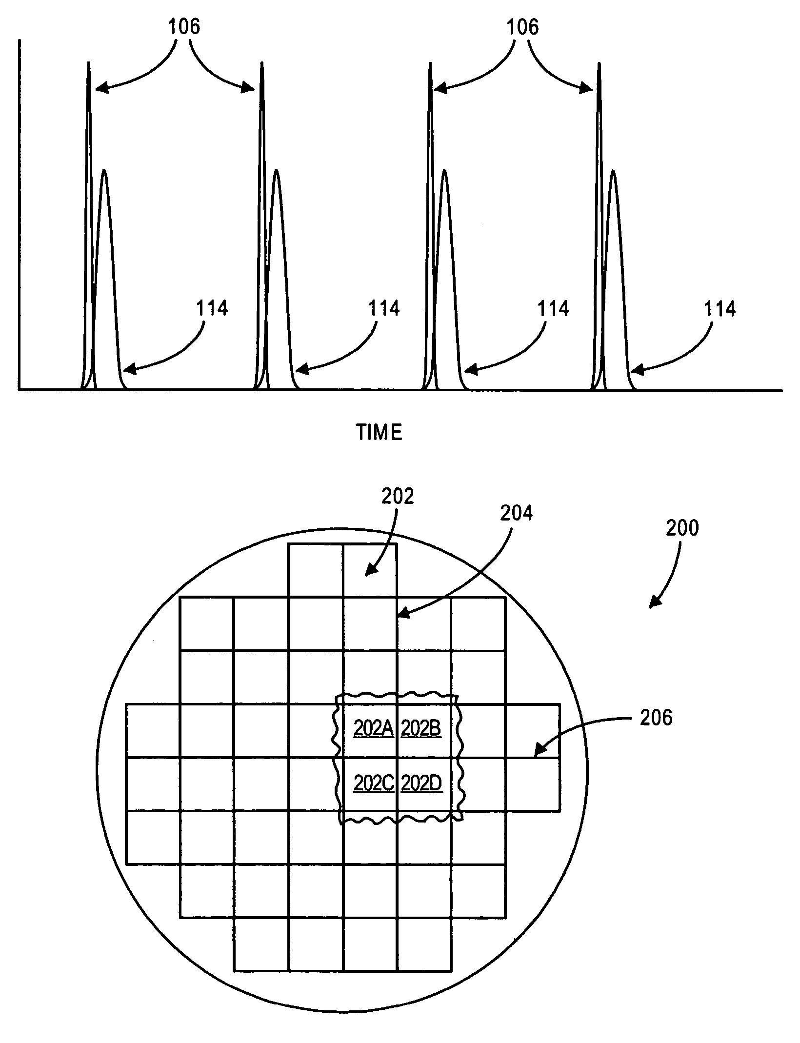
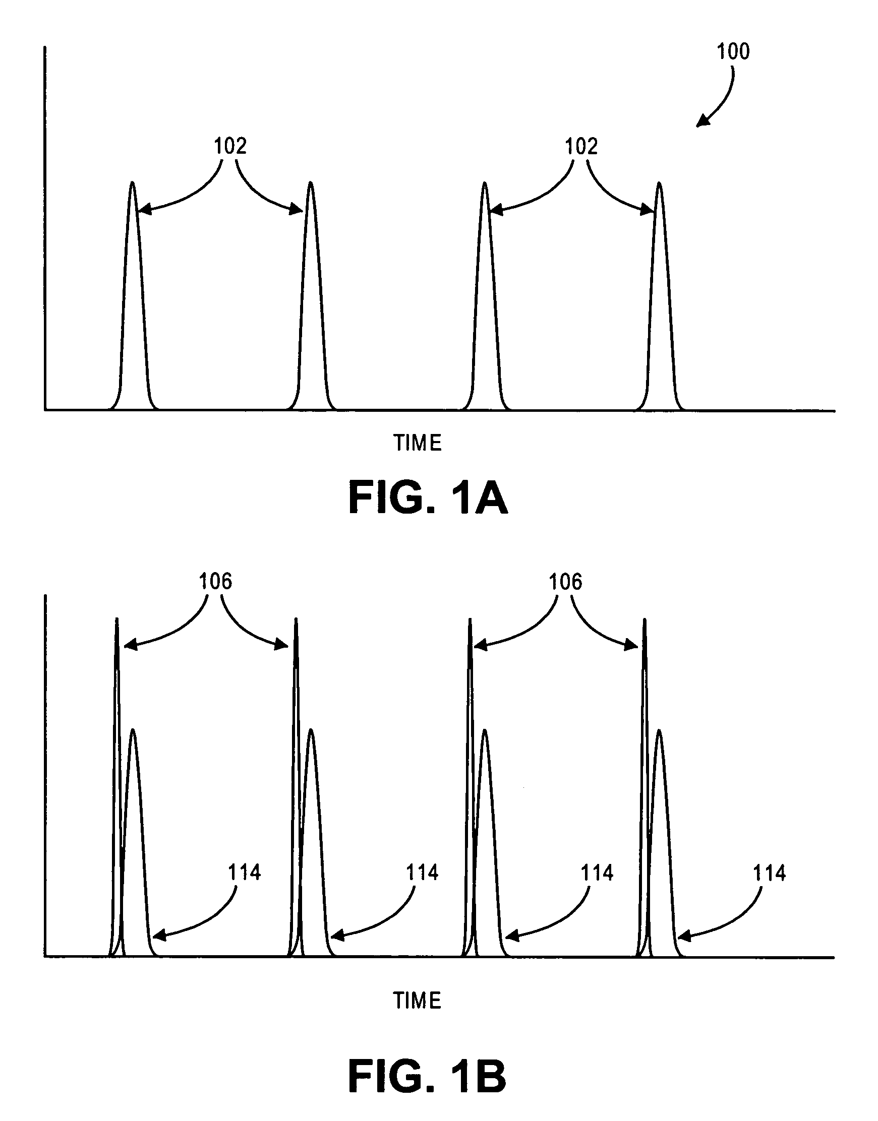
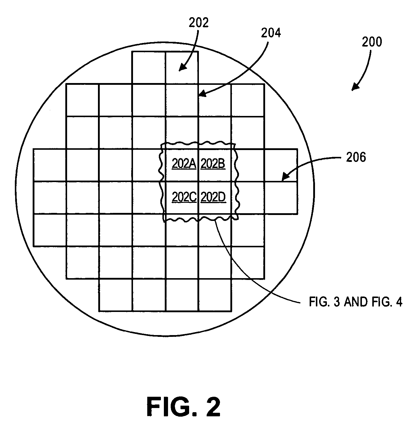
[0014]In the following detailed description, a method for laser micromachining a workpiece is disclosed. Reference is made to the accompanying drawings within which are shown, by way of illustration, specific embodiments by which the present invention may be practiced. It is to be understood that other embodiments may exist and that other structural changes may be made without departing from the scope and spirit of the present invention.

[0015]Embodiments of the present invention relate generally to the concept of lowering the ablation threshold of a material to facilitate its ablation at reduced power levels. More specifically, embodiments of the present specification disclose a dual source process whereby a first energy source lowers the ablation threshold of a material so a second energy source can ablate it at a lower power level than would otherwise be possible. While embodiments herein disclose the use of lasers, one of ordinary skill appreciates that these embodiments are not ...


PUM

PropertyMeasurementUnit
wavelengthaaaaaaaaaa

Abstract

A method is described for laser scribing or dicing portions of a workpiece using multi-source laser systems. In one embodiment, a first laser uses multiphoton absorption to lower the ablation threshold of portions of the workpiece prior to a second laser ablating the portions of the workpiece. In an alternative embodiment, a first laser uses high energy single-photon absorption to lower the ablation threshold of portions of the workpiece prior to a second laser ablating the portions of the workpiece.

Description

FIELD OF THE INVENTION [0001]Embodiments of the present invention relate generally to micromachining and more specifically to laser micromachining of semiconductor substrates.RELATED APPLICATIONS[0002]The present application is related to the subject matter of U.S. patent application Ser. No. 10 / 972,108 of Li entitled “Laser Micromachining Method,” and filed Oct. 21, 2004. U.S. patent application Ser. No. 10 / 972,108 is assigned to the assignee hereof.FIELD OF THE INVENTION[0003]Embodiments of the present invention relate generally to micromachining and more specifically to laser micromachining of semiconductor substrates.BACKGROUND OF THE INVENTION[0004]Semiconductor wafer singulation is typically accomplished using saws. However, sawing may not be suitable for cutting through advanced-materials formed on the wafer surface (i.e., low-k dielectrics). One alternative includes using lasers to remove scribe line material prior to sawing. Laser scribing, however, is confronted with a num...

Claims


Application Information

Patent Timeline
Patent Type & Authority Patents(United States)
IPC IPC(8): H01L21/00
CPCB23K26/063B23K26/4075B23K26/0635B23K2201/40B23K26/0622B23K26/0624B23K26/40B23K2101/40B23K2103/50
Inventor LI, ERIC J.VORONOV, SERGEI L.RUMER, CHRISTOPHER L.
Owner INTEL CORP
Why Eureka
Try Eureka