Substrate processing apparatus

Inactive Publication Date: 2006-05-04
TOYODA KAZUYUKI +6
View PDF9 Cites 20 Cited by
  • Summary
  • Abstract
  • Description
  • Claims
  • Application Information

AI Technical Summary

Benefits of technology

[0018] It is, therefore, a major object of the present invention to provide a substrate processing appa

Problems solved by technology

A plant for manufacturing semiconductor devices which r

Method used


Image

  • Substrate processing apparatus
  • Substrate processing apparatus
  • Substrate processing apparatus

Examples


first embodiment

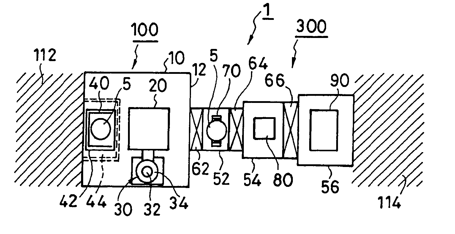
[0059] Referring to FIG. 1A to 9, a semiconductor wafer processing apparatus 1 will be explained by taking the case of a plasma CVD apparatus.

[0060] The semiconductor wafer processing apparatus 1 includes a cassette loader unit 100 and two connection modules 300.

[0061] The cassette loader unit 100 includes a cassette loader chamber 10 having a chamber wall 12 to which the two connection modules 300 are respectively detachably attached. The two connection modules 300 are piled up at a distance in a vertical direction.

[0062] Because the plurality of connection modules 300 are piled up in a vertical direction in this manner, even though the processing efficiency of the wafers 5 is enhanced by using the plurality of connection modules 300, the space occupied in a clean room by the semiconductor wafer processing apparatus 1 is not increased.

[0063] Further, maintenance areas of the semiconductor wafer processing apparatus 1 are only a maintenance area 112 at the side of the cassette l...

second embodiment

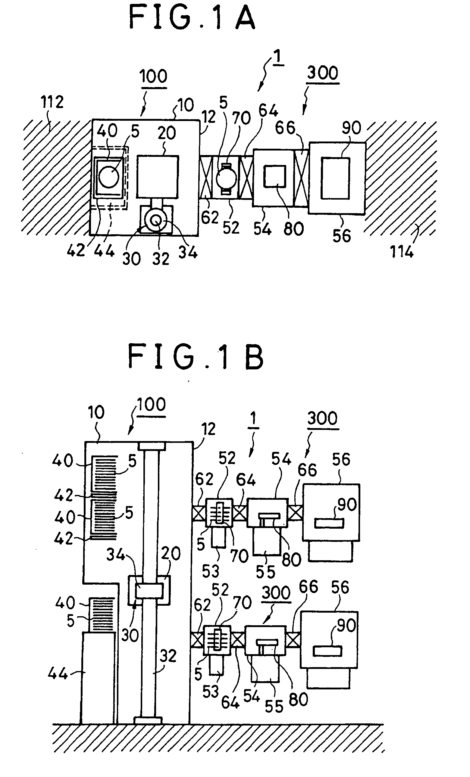
[0105]FIGS. 12A and 12B are views for explaining a semiconductor wafer processing apparatus according to the present invention, wherein FIG. 12A is a plan view and FIG. 12B is a sectional view.

[0106] In the above described first embodiment, the gate valve 64 is provided between the load lock chamber 52 and the transfer chamber 54. In the second embodiment, such a gate valve is not provided, and the wafer boat 70 and the wafer transfer robot 80 are provided in a common load lock-cum-transfer chamber 58. Other structure is the same as that of the first embodiment.

third embodiment

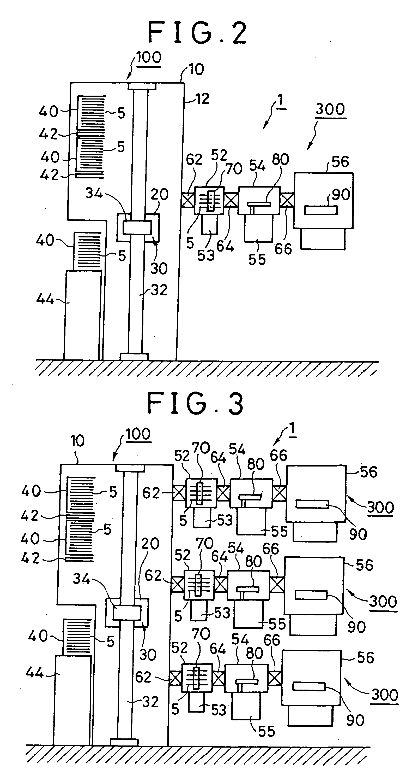
[0107] A third embodiment will be explained while taking the case of a plasma CVD apparatus for forming a nitride film or oxide film on a wafer, as a semiconductor wafer processing apparatus 2.

[0108]FIGS. 13A and 13B are views for explaining a semiconductor wafer processing apparatus according to the third embodiment of the invention, wherein FIG. 13A is a plan view, and FIG. 13B is a sectional view. FIGS. 14 and 15 are sectional views and FIGS. 16 to 19 are plan views, all for explaining the semiconductor wafer processing apparatus of the third embodiment.

[0109] The semiconductor wafer processing apparatus 2 comprises: a cassette loader unit 100 in which the elevator 30 and the cassette transferring-cum-wafer transferring robot 20 capable of transferring the wafers 5 vertically and horizontally; gate valves 462 and 464 for opening and closing a gate of each of connection modules 400; a load lock-cum-transfer chamber 452 which is provided therein with a wafer transfer robot 480 for...


PUM


Abstract

A substrate processing apparatus comprises a substrate transfer section, a plurality of modules and a first substrate transfer robot provided in the substrate transfer section and capable of transferring substrates to the plurality of modules. The plurality of modules are piled up, separately from one another, in a vertical direction. Each of the plurality of modules are detachably mounted to the substrate transfer section and includes a substrate processing chamber, an intermediate chamber, a first gate valve disposed between the substrate processing chamber and the intermediate chamber, a second gate valve disposed between the intermediate chamber and the substrate transfer section, and a second substrate transfer robot disposed in the intermediate chamber. Preferably, the substrate processing chamber further comprises a second intermediate chamber having a substrate holder therein and disposed between the intermediate chamber and the substrate transfer section, and a third gate valve disposed between the second intermediate chamber and the substrate transfer section.

Description

CROSS REFERENCE TO RELATED APPLICATIONS [0001] This application is a Continuation of co-pending application Ser. No. 08 / 905,971, filed on Aug. 5, 1997, for which priority is claimed under 35 U.S.C. § 120. Application Ser. No. 08 / 905,971 claims priority under 35 U.S.C. § 119(a)-(d) from Application No. 8-223076 filed in Japan on Aug. 5, 1996. The entire contents of each of the above-identified applications are hereby incorporated by reference.BACKGROUND OF THE INVENTION [0002] 1. Field of the Invention [0003] The present invention relates to a substrate processing apparatus, more particularly, to a semiconductor wafer processing apparatus, and still more particularly, to a semiconductor wafer processing apparatus for processing a semiconductor wafer utilizing plasma, such as a plasma enhanced etching apparatus, a plasma enhanced CVD (Chemical Vapor Deposition) apparatus and a plasma enhanced ashing apparatus. [0004] 2. Description of the Related Art [0005]FIG. 20 shows an example of ...

Claims


Application Information

Patent Timeline
IPC IPC(8): C23F1/00C23C16/54H01L21/00H01L21/677
CPCC23C16/54H01L21/67178H01L21/67766H01L21/67781H01L21/67161C23C16/50
Inventor TOYODA, KAZUYUKISUDA, ATSUHIKOMAKIGUCHI, ISSEITANAKA, TSUTOMUSUZUKI, SADAYUKINOMURA, SHINICHITAKESHITA, MITSUNORI
Owner TOYODA KAZUYUKI
Why Eureka
Try Eureka