Semiconductor device and its manufacture method

a technology of semiconductor devices and manufacturing methods, applied in semiconductor devices, electrical devices, transistors, etc., can solve the problems of not teaching the mixture of memory circuits and peripheral circuits, and the requirement of using the same wiring structure is difficult to be met, and achieves high performance.

Inactive Publication Date: 2006-05-04
FUJITSU SEMICON LTD
View PDF2 Cites 12 Cited by
  • Summary
  • Abstract
  • Description
  • Claims
  • Application Information

AI Technical Summary

Benefits of technology

[0030] An object of the present invention is to provide a semiconductor device of high performance having crossed wirings suitable for miniaturization.

Problems solved by technology

This publication does not teach mixture of a memory circuit and a peripheral circuit.
These requirements are hard to be met by using the same wiring structure.

Method used


Image

  • Semiconductor device and its manufacture method
  • Semiconductor device and its manufacture method
  • Semiconductor device and its manufacture method

Examples


first embodiment

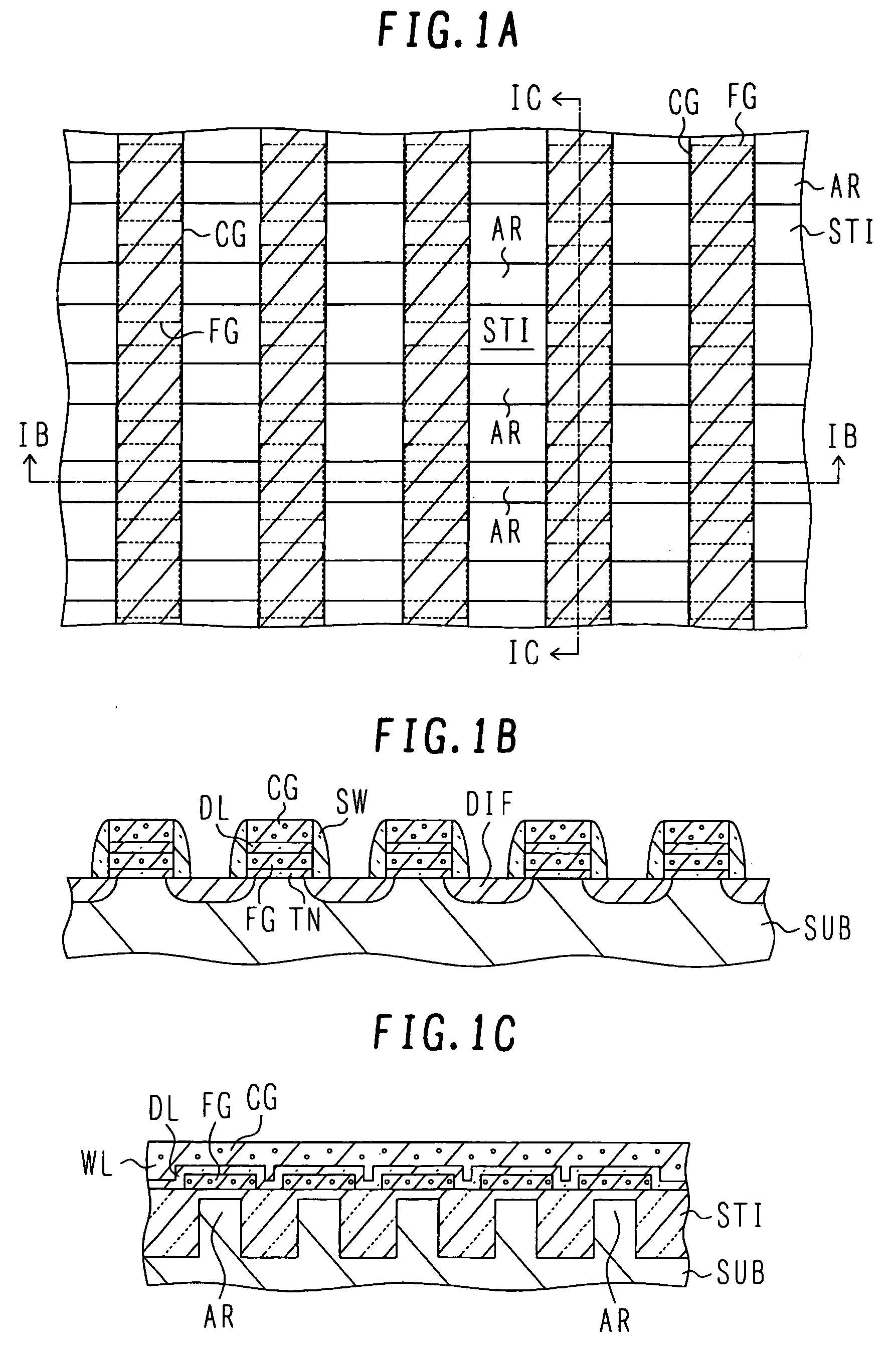
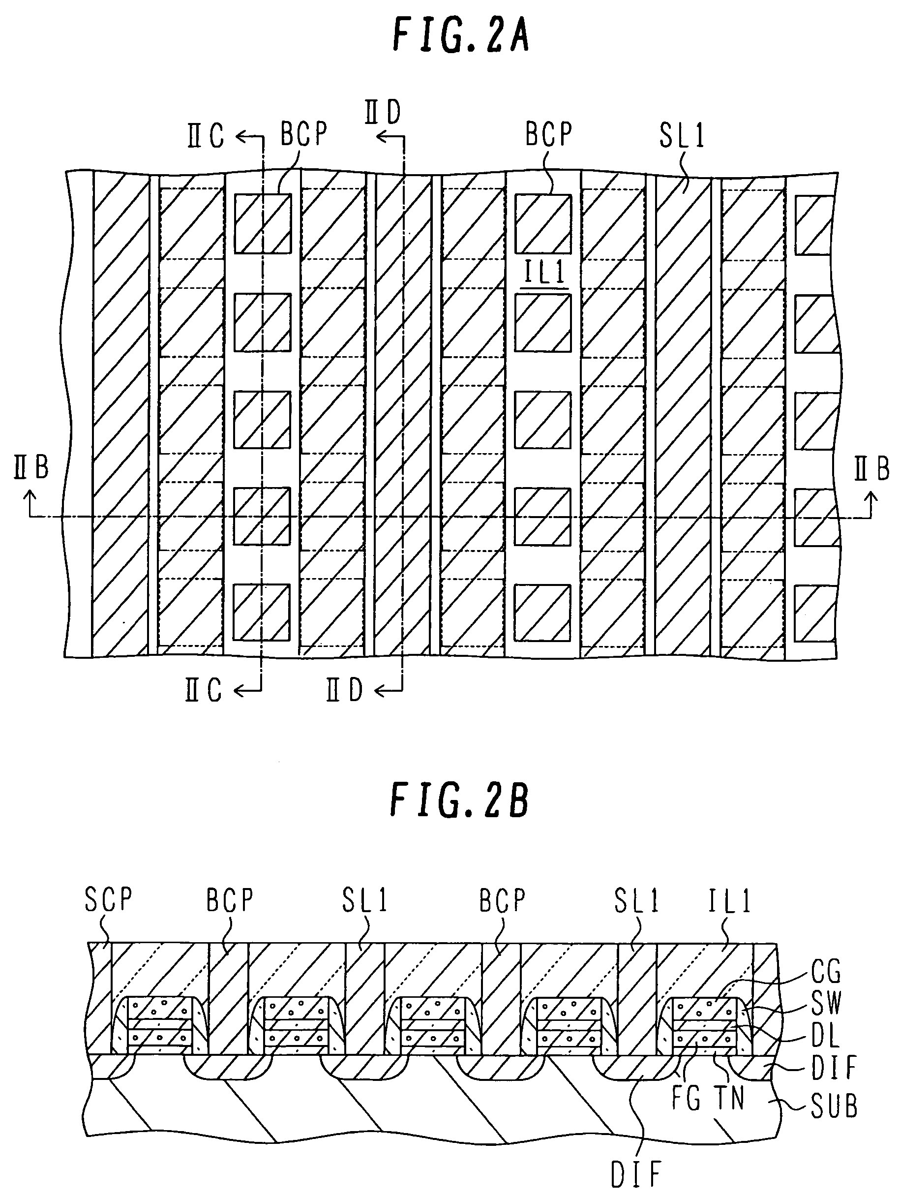
[0049]FIGS. 1A to 3H are plan views and cross sectional views showing the structure of the semiconductor device according to the present invention. FIGS. 1A, 1B and 1C show a lower layer structure in which transistors constituting flash memory cells are formed on a semiconductor substrate. FIGS. 2A to 2D show a middle layer structure in which a first interlayer insulating film is formed on the lower layer structure and plugs are buried in the first interlayer insulating film. FIGS. 3A to 3H show a semiconductor device having wirings formed on the middle layer structure.

[0050] As shown in FIG. 1A, an element isolation region STI is formed in a semiconductor substrate by shallow trench isolation to define a plurality of striped active regions AR. A gate structure (word line structure) including a floating gate FG and a control gate CG is formed crossing the active regions AR.

[0051]FIG. 1B is a cross sectional view of an active regions taken along line IB-IB shown in FIG. 1A. A gate s...

second embodiment

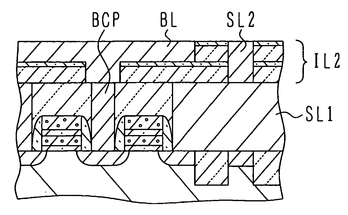
[0119]FIG. 9B illustrates the case wherein the second source line is formed. A silicon oxide layer 41 is formed on a control gate electrode layer 8 of polysilicon, and side wall spacers 10 are formed on the side walls of the gate electrode to constitute a gate electrode structure. Similar to the second embodiment, a first interlayer insulating film IL1 is formed covering the gate electrode structures.

[0120] At the same time when the first source lines and bit contact plugs are formed, the third source line SL3 crossing the gate electrode structures is formed covering the gate electrode structure. The third source line SL3 electrically connects the plurality of first source lines.

[0121] On the third source line SL3, the second source line SL2 similar to that of the above-described embodiments is formed. The second and third source lines SL2 and SL3 in unison connect the plurality of first source lines SL1 at a low resistance to provide a ground source line having a low resistance as...


PUM


Abstract

A semiconductor device includes: a first insulating layer with a flat surface formed over a semiconductor substrate structure in which a plurality of semiconductor elements are formed; column-like conductive plugs formed to penetrate the first insulating layer in the thickness direction; elongated wall-like conductive plugs formed through the first insulating layer in the thickness direction; a second insulating layer with a flat surface formed on the first insulating layer covering the column-like conductive plugs and the wall-like conductive plugs; and first wirings having dual damascene structures. Each of the first wirings has a first portion penetrating the second insulating layer in the thickness direction and connected to at least one of the columnar conductive plugs, and a second portion formed in the second insulating layer to an intermediate depth and apparently intersects at least one of the wall-like conductive plugs when viewed above.

Description

CROSS REFERENCE TO RELATED APPLICATION [0001] This application is based on and claims priority of PCT / JP2003 / 011125 filed on Aug. 29, 2003, the entire contents of which are incorporated herein by reference.BACKGROUND OF THE INVENTION [0002] A) Field of the Invention [0003] The present invention relates to a semiconductor device and its manufacture method, and more particularly to a semiconductor device having crossing cubic wirings and its manufacture method. [0004] B) Description of the Related Art [0005] As an integration degree of semiconductor devices is improved, wirings are becoming finer. An integration degree of lower layer wirings near a semiconductor substrate is particularly high and there is high demands for miniaturization. Even if wirings are made fine, it is desired to lower parasitic resistance and parasitic capacitance. Various proposals have been made for lowering parasitic resistance and capacitance. [0006] A conductive plug is formed by forming an insulating film...

Claims


Application Information

Patent Timeline
Patent Type & Authority Applications(United States)
IPC IPC(8): H01L29/76H01L21/8247H01L27/105H01L27/115H01L29/788H01L29/792
CPCH01L27/105H01L27/115H01L27/11526H01L27/11529H10B69/00H10B41/40H10B41/41
Inventor EMA, TAIJI
Owner FUJITSU SEMICON LTD
Why Eureka
Try Eureka