

Thin film probe sheet and semiconductor chip inspection system
- Summary
- Abstract
- Description
- Claims
- Application Information
AI Technical Summary
Benefits of technology
Problems solved by technology
Method used
Image

Examples
first embodiment
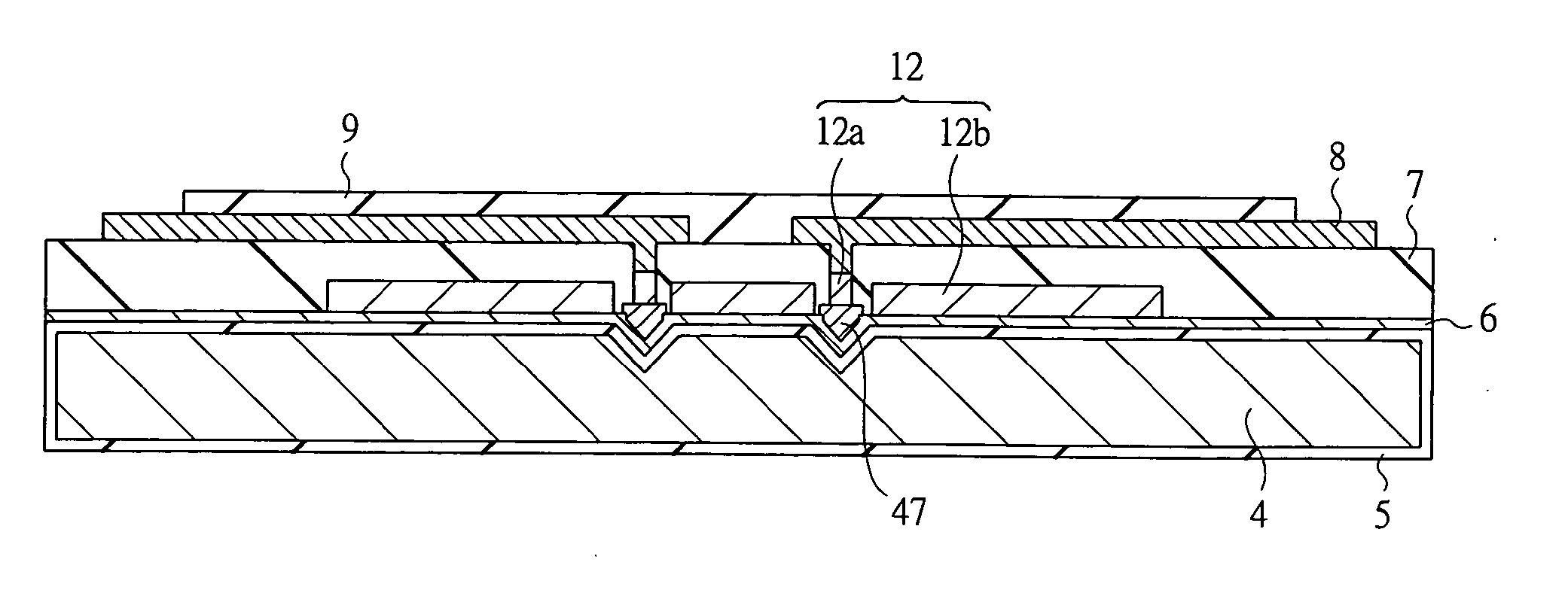
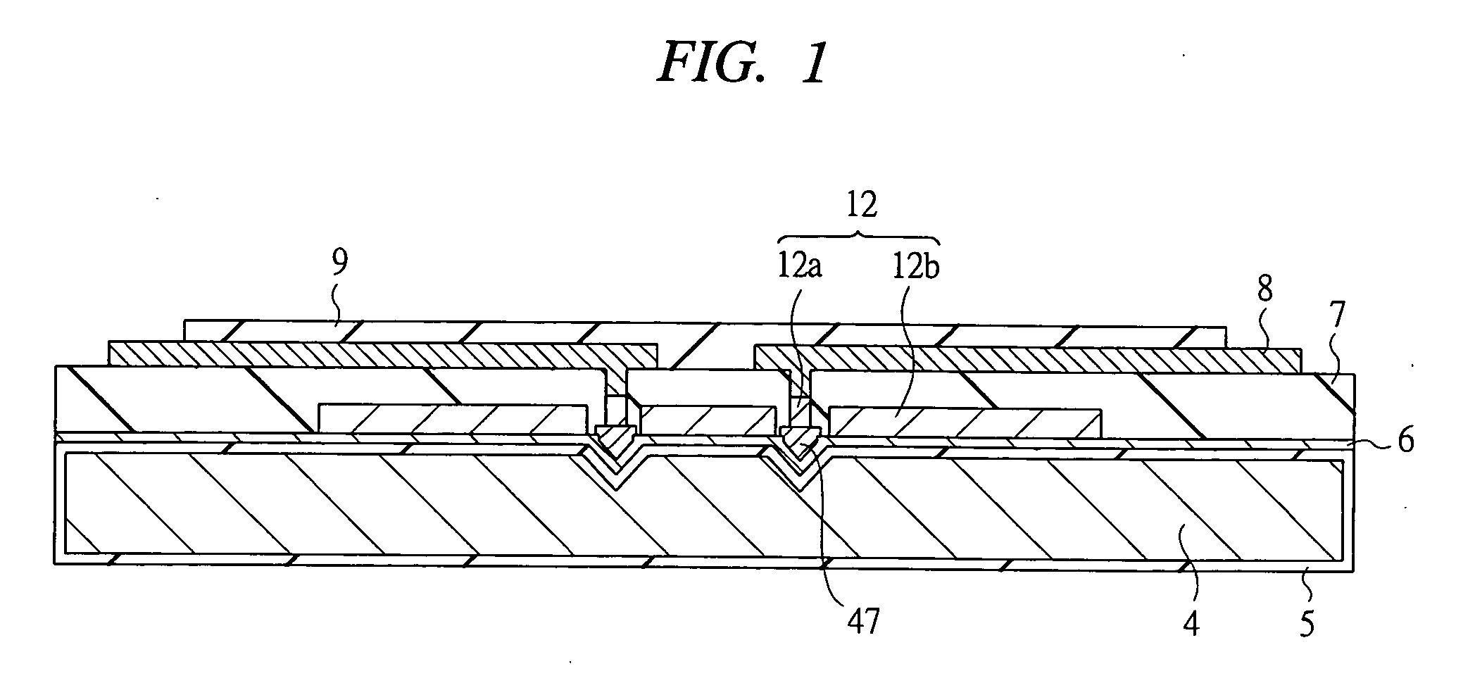
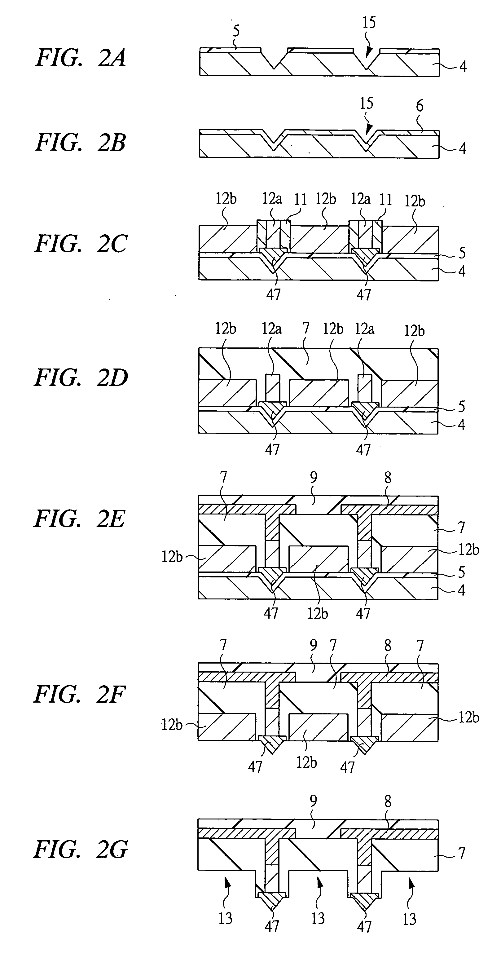
[0093]FIG. 1 is a drawing of the entire cross-sectional structure of a thin film probe sheet according to a first embodiment of the present invention. FIG. 2A to FIG. 2G are explanatory drawings illustrating the manufacturing process of the thin film probe sheet of FIG. 1. FIG. 3 is an explanatory drawing illustrating the relation between the cross-sectional structure and the outline shape of the thin film probe sheet of FIG. 1. FIG. 4 is a cross-sectional schematic drawing illustrating the detailed structure of the contact terminals in the part A of FIG. 3.
[0094] In the first embodiment, FIG. 1 and FIG. 2 illustrate the manufacturing process of the thin film probe sheet. FIG. 1 illustrates the structure of the thin film probe sheet which is completed through the thin film process on a silicon substrate serving as a base material, and FIG. 2 is a detailed flowchart of the manufacturing process.
[0095] For a 100 plane of the silicon substrate 4 which is a single crystal silicon wafe...
second embodiment
[0115]FIG. 5 is a schematic drawing of the cross section showing the outline of the plating deposition properties to a silicon mold hole for a contact terminal according to a second embodiment of the present invention.
[0116] In the second embodiment, the manufacturing process for further narrowing pitches in a thin film probe sheet having the basically same structure as that obtained by the manufacturing process shown in the above-described first embodiment will be described with reference to FIG. 5.
[0117] The process for manufacturing a thin film probe sheet includes: the steps in which the mold holes 15 formed by the anisotropic etching of the silicon substrate 4 which is a single crystal silicon wafer are filled with the hard metal film 30 and the subsidiary metal film 31 constituting the contact terminals 47 by electroplating, and the dummy metal film 12 formed as a means for extending the terminal height is similarly disposed in the adjacent region by electroplating; and the ...
third embodiment
[0125]FIG. 6A to 6D are structural drawings showing arrangement of a thin film probe sheet of a third embodiment of the present invention and electrode pads of a semiconductor device for a liquid crystal display panel. FIGS. 7A and 7B are a plan view showing the relation in the arrangement of the electrode pads and the contact terminals of the third embodiment of the present invention and a schematic drawing of a cross section showing the plating deposition state of the electrode pad of the semiconductor device in which an Au bump is formed.
[0126] In the third embodiment, an example of the structure of the thin film probe sheet and a semiconductor chip 2 which is an inspection target is shown in FIG. 6A to FIG. 6D.
[0127]FIG. 6A and FIG. 6B are the plan view and the cross-sectional view of the entire sheet shown in FIG. 3, FIG. 6C shows a cross section showing the relation of the electrode pads 3 of the semiconductor chip 2 which is an inspection target facing to the contact termin...
PUM
| Property | Measurement | Unit |
|---|---|---|
| thickness | aaaaa | aaaaa |
| depth | aaaaa | aaaaa |
| depth | aaaaa | aaaaa |
Abstract
Description
Claims
Application Information