Apparatus for manufacturing an electronic device, method of manufacturing an electronic device, and program for manufacturing an electronic device

a technology for electronic devices and manufacturing methods, applied in the direction of soldering apparatus, manufacturing tools, printed circuit non-printed electric components association, etc., can solve the problems of reducing the use of space, restricting the deterioration of product quality in reflow treatment, and poor production efficiency, so as to achieve efficient manufacturing of electronic devices

Inactive Publication Date: 2006-05-11
SEIKO EPSON CORP
View PDF7 Cites 3 Cited by
  • Summary
  • Abstract
  • Description
  • Claims
  • Application Information

AI Technical Summary

Benefits of technology

[0018] As a result, it is possible to perform the electronic component mounting treatment and reflow treatment at one time while the continuous body is retracted, so that it is possible to avoid the unnecessary process of re-winding the continuous body where the electronic components are mounted and performing the reflow treatment, reduce the number of transports of the tape substrate, eliminate the process of tacking the electronic components and improve the production efficiency.
[0145] Therefore, it is possible to integrally perform the conductive material applying treatment, resin sealing treatment and cutting-out treatment of circuit blocks by the installation of the program for manufacturing an electronic device, and simultaneously perform a plurality of treatments on the continuous body where circuit blocks are placed in a line, so as to efficiently manufacture an electronic device.

Problems solved by technology

However, there have been problems in the apparatus for manufacturing an electronic device according to the prior art in that, as transport tacts are not uniform at the solder applying zone 122, mounting zone 132 and reflow zone 142, in order to perform the solder printing, and mounting and reflow of electronic components to one tape substrate 220, it is necessary to transport one tape substrate 220 three times between loaders 121, 131, 141 and unloaders 141, 142, 143, respectively, and the production efficiency is poor.
Therefore, it is possible to restrict thermal damage to the area to be heated by refracting the heat generating means from the area to be heated by a sufficient distance to insert a heat shielding plate between the heat generating means and the area to be heated, reduce the use of space, and restrict the deterioration of product quality in the reflow treatment.

Method used


Image

  • Apparatus for manufacturing an electronic device, method of manufacturing an electronic device, and program for manufacturing an electronic device
  • Apparatus for manufacturing an electronic device, method of manufacturing an electronic device, and program for manufacturing an electronic device
  • Apparatus for manufacturing an electronic device, method of manufacturing an electronic device, and program for manufacturing an electronic device

Examples


first embodiment

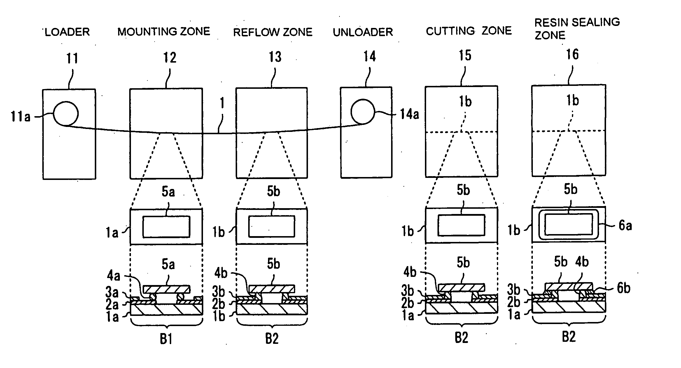
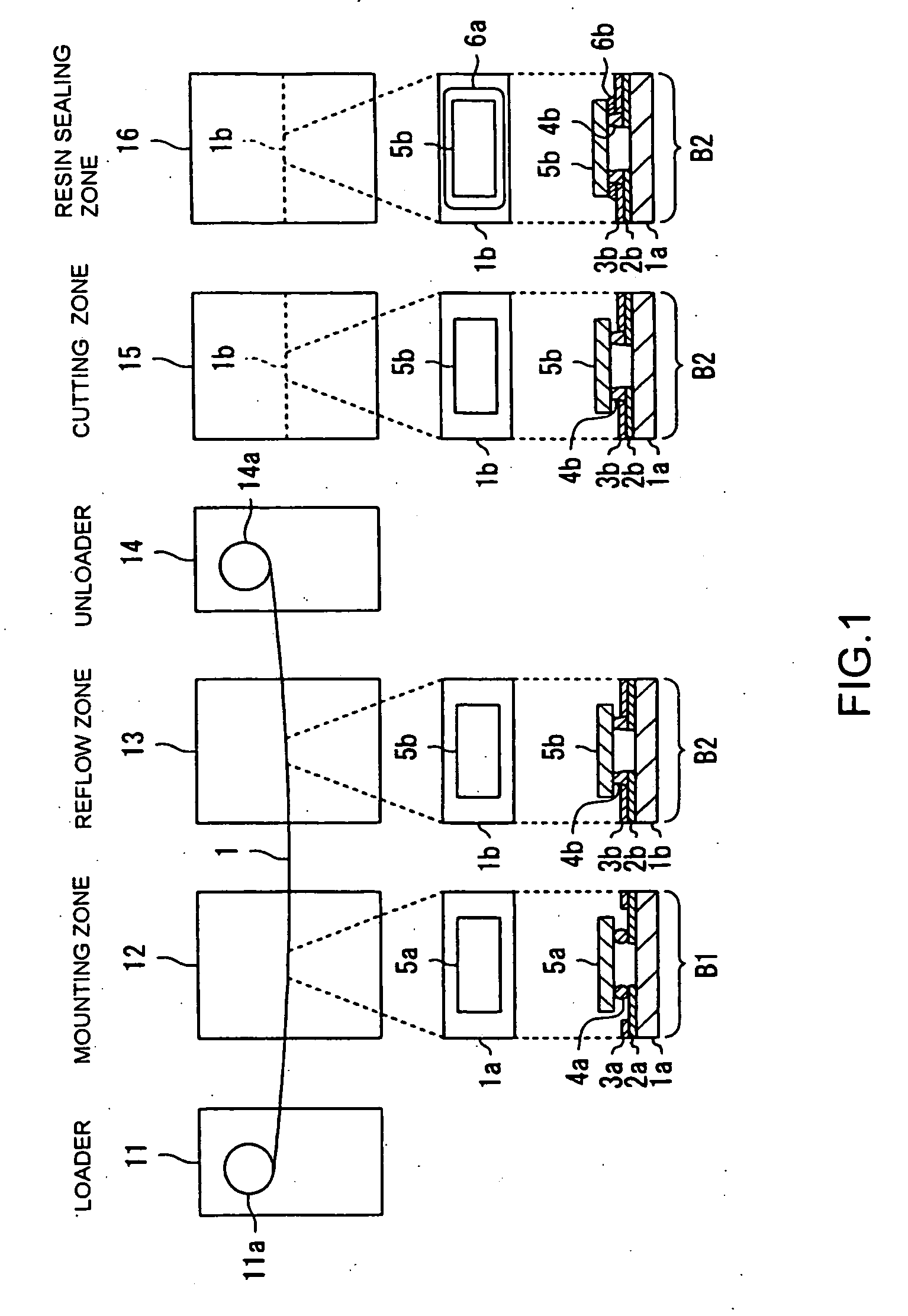
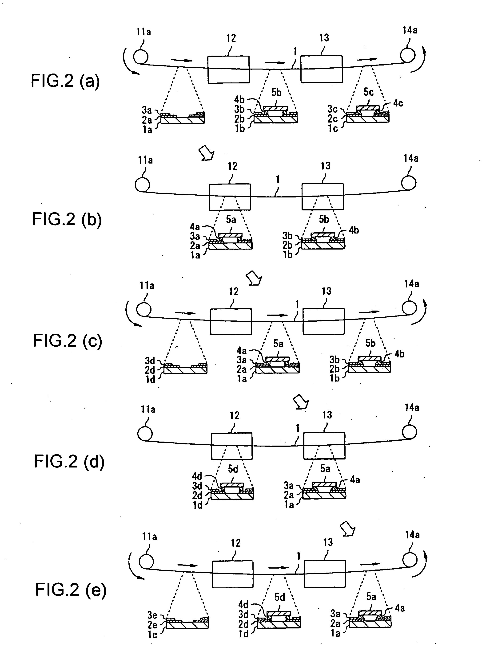
[0176]FIG. 2 is a diagram for illustrating an electronic device manufacturing process according to the present invention;

[0177] In FIG. 2(a), circuit substrates 1a to 1c are formed on the tape substrate 1 retracted between the unwinding reel 11a and a take-up reel 14a. At this time, a wiring 2a and an insulating film 3a are formed on the circuit substrate 1a. A wiring 2b and an insulating film 3b are formed on the circuit substrate 1b, and a semiconductor chip 5b where the soldering material ball 4b is formed is mounted on the circuit substrate 1b, a wiring 2c and an insulating film 3c are formed on the circuit substrate 1c, and a semiconductor chip 5c is fixed via the soldering material ball 4c. Moreover, in the tape substrate 1, with the circuit substrate 1a to 1c retracted, according to a predetermined transport tact, the circuit substrate 1a to which the mounting treatment has not been performed yet is transported to the mounting zone 12, and the circuit substrate 1b to which th...

second embodiment

[0184]FIG. 3 is a diagram for illustrating a method of manufacturing an electronic device according to the present invention.

[0185] In FIG. 3, a solder applying zone 22, a mounting zone 23 and a reflow zone 24 are arranged consecutively in parallel between a loader 21 and an unloader 25 along the transport direction of a tape substrate 31.

[0186] On the other hand, an electronic component mounting area is provided at each of circuit blocks B11 to B13 in the tape substrate 31, and circuit substrates 31a to 31c are respectively provided in the circuit blocks B11 to B13. Furthermore, wirings 32a to 32c are respectively formed on the circuit substrates 31a to 31c, and insulating films 33a to 33c are formed on the wirings 32a to 32c by the exposure of the terminals thereof.

[0187] Moreover, the tape substrate 31 where a predetermined length of circuit substrates 31a to 31c are placed in line is hung between an unwinding reel 21a and a take-up reel 25a. A solder unapplied area of the tape...

third embodiment

[0192]FIG. 4 is a diagram for illustrating a method of manufacturing an electronic device according to the present invention.

[0193] In FIG. 4, a solder applying zone 42, a mounting zone 43, a reflow zone 44, a resin applying zone 45 and a curing zone 4 are arranged between a loader 41 and an unloader 47 along the transport direction of a tape substrate 51.

[0194] An electronic component mounting area is provided at each of circuit blocks B21 to B25 in the tape substrate 51, and circuit substrates 51a to 51e are respectively provided on the circuit blocks B21 to B25. Furthermore, wirings 52a to 52e are respectively formed on the circuit substrates 51a to 51e, and insulating films 53a to 53e are formed on the wirings 52a to 52e by the exposure of the terminals thereof.

[0195] Moreover, the tape substrate 51 where a predetermined length of circuit substrates 51a to 51e are placed in line is hung between an unwinding reel 41a and a take-up reel 47a. A solder unapplied area of the tape s...


PUM

PropertyMeasurementUnit
lengthaaaaaaaaaa
lengthaaaaaaaaaa
lengthaaaaaaaaaa

Abstract

A mounting zone and a reflow zone are arranged in parallel between a loader and an unloader, and mounting and reflow processes are performed simultaneously.

Description

CROSS-REFERENCE TO RELATED APPLICATIONS [0001] This application is a divisional of U.S. patent application Ser. No. 10 / 394,478 filed Mar. 21, 2003, claiming priority to JP2002-081220 filed Mar. 22, 2002, JP2002-081221 filed Mar. 22, 2002, JP2002-081222 filed Mar. 22, 2002, JP2002-081223 filed Mar. 22, 2002, JP2002-084347 filed Mar. 25, 2002, and JP2003-024649 filed Jan. 31, 2003. The disclosures of the above applications are incorporated herein by reference.BACKGROUND OF THE INVENTION [0002] 1. Technical Field of the Invention [0003] The present invention relates to an apparatus, a method, and a program for manufacturing an electronic device, and more particularly to a soldering reflow process for a tape substrate, or the like on which electronic components are mounted. [0004] 2. Description of the Related Art [0005] Generally, if semiconductor chips are mounted on a circuit substrate of a COF (Chip On Film) module, a TAB (Tape Automated Bonding) module, or the like in a conventiona...

Claims


Application Information

Patent Timeline
Patent Type & Authority Applications(United States)
IPC IPC(8): B32B37/00B32B38/04H05K3/34B23K1/008B23K3/00H01L21/50H01L21/60H01L21/68H05K1/18H05K3/00
CPCH01L2924/01078Y10T156/1085H01L2924/3025H05K1/189H05K3/0097H05K3/3494H05K2203/1545B23K1/008B23K2201/40H01L21/6835H01L2224/16Y10S438/907Y10T156/1084Y10T156/1052Y10T156/1343Y10T156/1751Y10T156/1097H01L2924/19041B23K2101/40H05K13/00
Inventor SHIOZAWA, MASAKUNI
Owner SEIKO EPSON CORP
Why Eureka
Try Eureka