Silicon carbide semiconductor device and method for manufacturing the same
- Summary
- Abstract
- Description
- Claims
- Application Information
AI Technical Summary
Benefits of technology
Problems solved by technology
Method used
Image

Examples
first embodiment
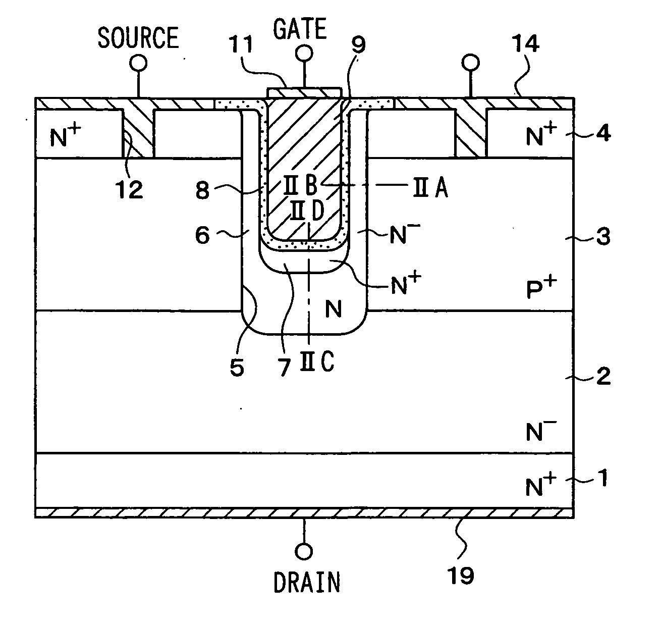
[0042]FIG. 1 shows a cross sectional view of a cell region of a trench type vertical power MOSFET as an accumulation type MOSFET according to a first embodiment of the present invention. The construction of the vertical power MOSFET shown in FIG. 1 is explained.
[0043] A N− type drift layer 2 is disposed on a N+ type substrate 1. A P+ type base region 3 and a N+ type source region 4 are formed on the surface of the N− type drift layer 2. In this embodiment, a semiconductor substrate is composed of the N+ type substrate 1, the N− type drift layer 2, the P+ type base region 3 and the N+ type source region 4.
[0044] A trench 5 is formed to penetrate the N+ type source region 4 and the P+ type base region 3 and to reach the N− type drift layer 2. A N− type channel layer 6 is formed on an inner wall of the trench 5. A N+ type low resistance layer 7 is formed on a surface portion of the N− type channel layer 6 disposed on the bottom of the trench 5.
[0045] An oxide film 8 is formed to cov...
second embodiment
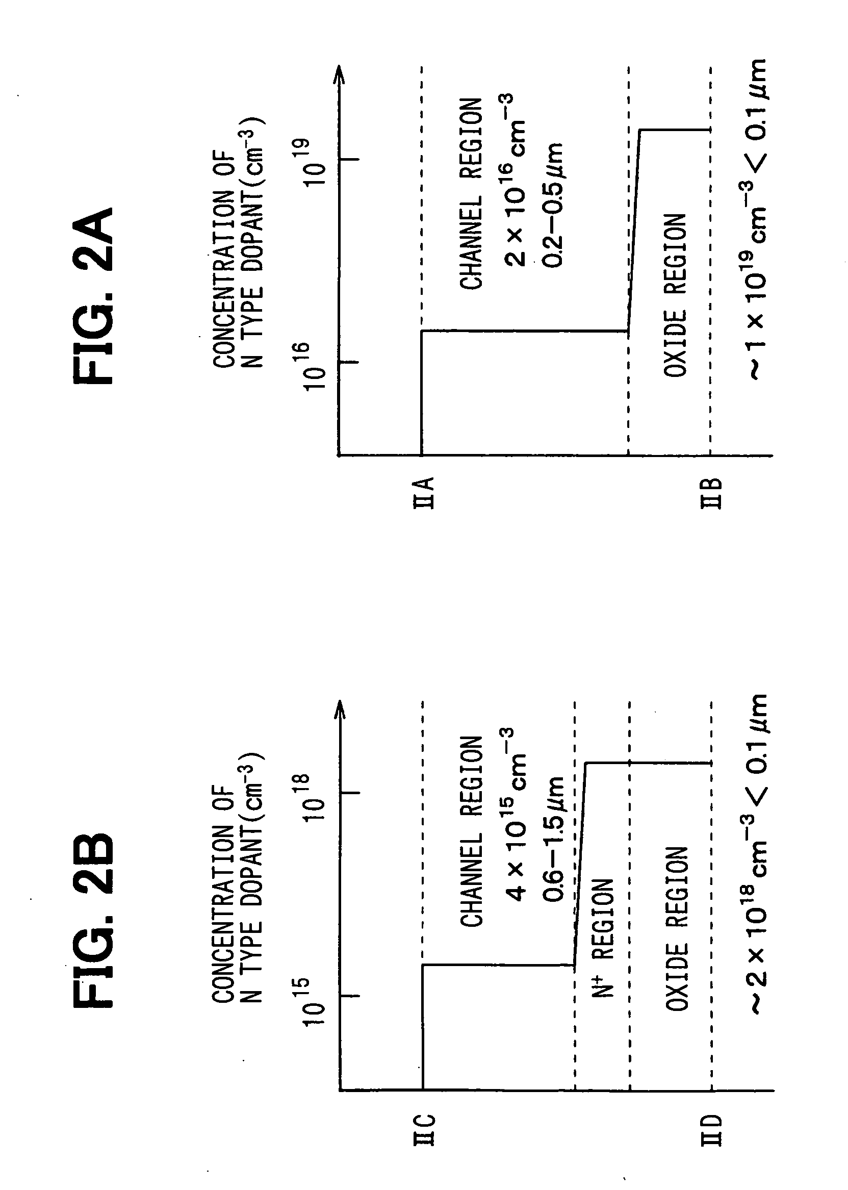
[0083] A second embodiment of the present invention is explained as follows. FIG. 11A is a cross sectional view showing a MOSFET as a silicon carbide semiconductor device according to this embodiment. FIG. 11B is a profile of a dopant concentration of a P conductive type impurity in the MOSFET along line XIE-XIF shown in FIG. 11A. The MOSFET according to this embodiment is explained with reference to FIGS. 11A and 11B as follows. The basic construction of the MOSFET according to this embodiment is similar to the first embodiment. Therefore, only the difference between them is explained.
[0084] In the second embodiment of the present invention, similar to the first embodiment, the P+ type base region 3 disposed on both sides of the trench 5 is arranged to be disposed on a lower side of the utmost lowest position of the oxide film 8. The impurity concentration of the P type impurity in the P+ type base region 3 is gradually reduced from the height of the position corresponding to the ...
third embodiment
[0086] A third embodiment of the present invention is explained as follows. FIG. 12A is a cross sectional view showing a MOSFET as a silicon carbide semiconductor device according to this embodiment. FIG. 12B is a profile of a dopant concentration of a P conductive type impurity in the MOSFET along line XIIG-XIIH shown in FIG. 12A, and FIG. 12C is a profile of a dopant concentration of a N conductive type impurity in the MOSFET along line XIII-XIIJ shown in FIG. 12(a). The MOSFET according to this embodiment is explained with reference to FIGS. 12A to 12C as follows. The basic construction of the MOSFET according to this embodiment is similar to the first embodiment. Therefore, only the difference between them is explained.
[0087] In the third embodiment of the present invention, differently from the first embodiment, the construction includes no N+ type low resistance layer 7. Similar to the first embodiment, the P+ type base region 3 disposed on both sides of the trench 5 is arran...
PUM
 Abstract
Description
Claims
Application Information
 - R&D
- Intellectual Property
- Life Sciences
- Materials
- Tech Scout
- Unparalleled Data Quality
- Higher Quality Content
- 60% Fewer Hallucinations
Browse by: Latest US Patents, China's latest patents, Technical Efficacy Thesaurus, Application Domain, Technology Topic, Popular Technical Reports.
© 2025 PatSnap. All rights reserved.Legal|Privacy policy|Modern Slavery Act Transparency Statement|Sitemap|About US| Contact US: help@patsnap.com