Method for forming gate of semiconductor device

a technology of semiconductor devices and gate elements, applied in the direction of semiconductor devices, basic electric elements, electrical appliances, etc., can solve the problems of increasing leakage current, reducing threshold voltage, and crystal defects such as stacking faults, so as to prevent the characteristic and reliability of the device from being degraded

Active Publication Date: 2009-12-17
KEY FOUNDRY CO LTD
View PDF15 Cites 3 Cited by
  • Summary
  • Abstract
  • Description
  • Claims
  • Application Information

AI Technical Summary

Benefits of technology

[0017]An embodiment of the present invention is directed to providing a method for forming a gate of a semiconductor device, which is capable of preventing characteristic and reliability of the device from being degraded by a plasma etching process.
[0018]Another embodiment of the present invention is directed to providing a method for forming a gate of a semiconductor device, which is capable of preventing electric field concentration from occurring at an upper edge portion due to a plasma etching process.

Problems solved by technology

Thus, severe interference between the source and the drain causes a short channel effect that reduces a threshold voltage and increases leakage current.
However, in the method for forming the recess gate type transistor, since the substrate is etched by a plasma etching process, a region for channel is damaged by plasma, causing crystal defects such as stacking fault.
Furthermore, surface roughness is degraded due to characteristic of plasma etching.
Moreover, when a trench is formed by etching the substrate, an upper edge portion is formed sharply and an electric field is concentrated on the sharp upper edge portion, resulting in degradation in characteristic and reliability of the device.
First, crystal defect is caused by plasma damage.
If crystal defect caused by plasma damage occurs in the side A to be used as a channel, device characteristics are degraded.
In particular, the reliability of the device is degraded.
Second, the use of the plasma etching process degrades surface roughness such as striation that is inevitably formed in the side A during the plasma etching process.
Thus, failure of the gate oxide layer is caused, or the lifespan of the gate oxide layer is reduced.

Method used


Image

  • Method for forming gate of semiconductor device
  • Method for forming gate of semiconductor device
  • Method for forming gate of semiconductor device

Examples


embodiment 1

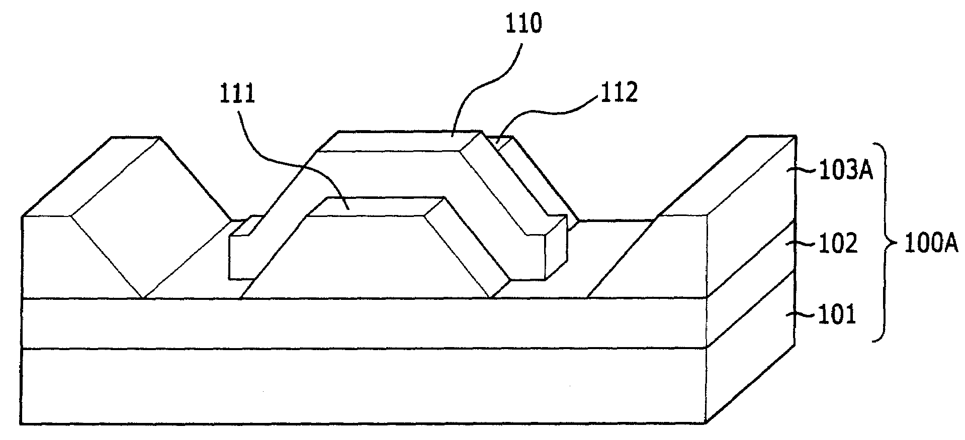
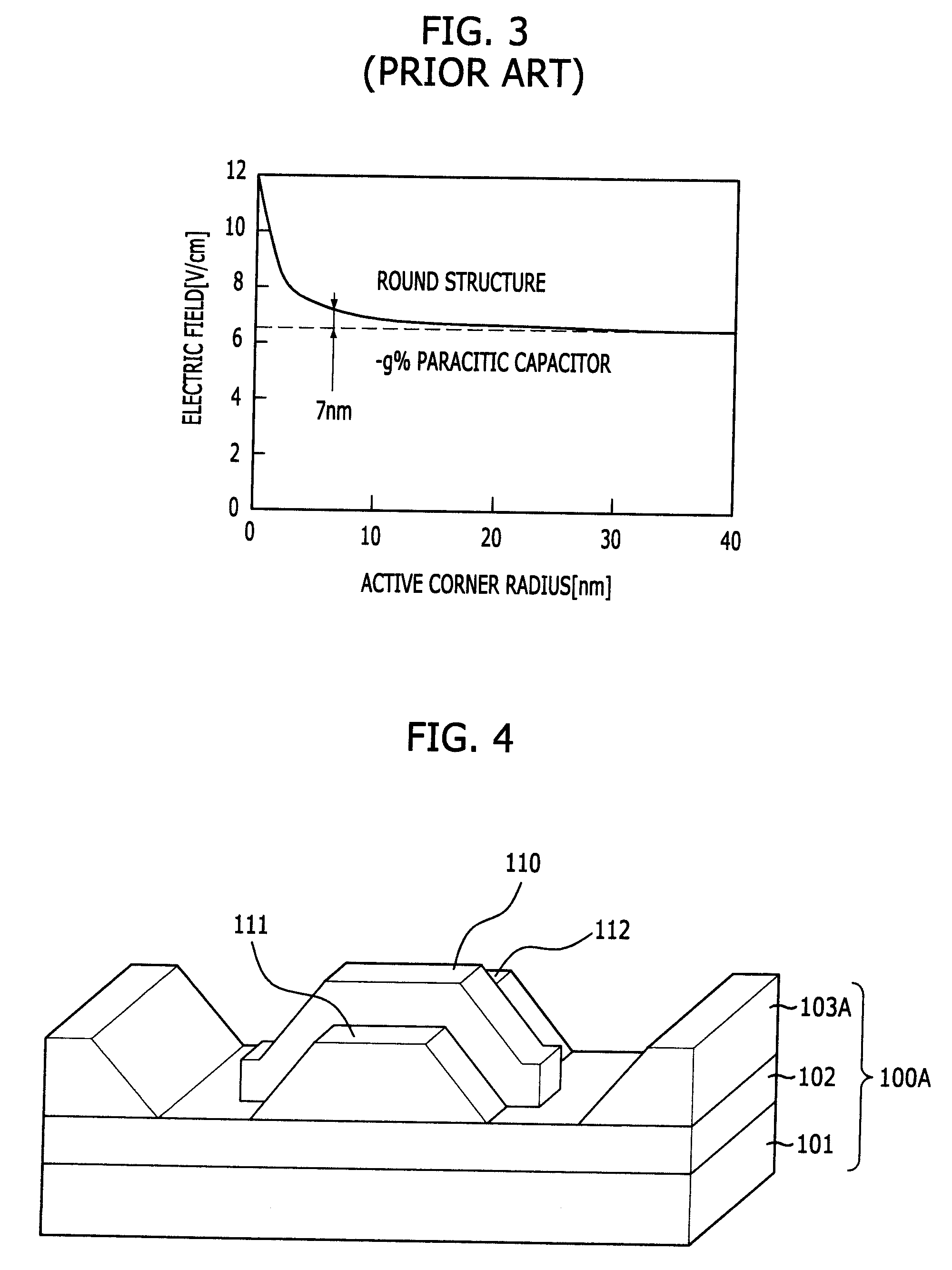
[0033]FIG. 4 is a perspective view of a triple gate formed by a method for forming a triple gate of a semiconductor device in accordance with a first embodiment of the present invention. FIGS. 5A to 5G are cross-sectional views illustrating a method for forming a triple gate of a semiconductor device in accordance with a first embodiment of the present invention.

[0034]Referring to FIG. 5A, a substrate 100 is prepared. The substrate 100 is a silicon-on-insulator (SOI) substrate and includes a support substrate 101, a buried insulation layer 102, and a semiconductor layer 103. The buried insulation layer 102 is formed of oxide to a thickness of approximately 100 Å or more, specifically, approximately 100 Å to approximately 1,000 Å. The semiconductor layer 103 is formed to a thickness of approximately 300 Å or more, specifically, approximately 300 Å to approximately 1,000 Å. The semiconductor layer 103 may include an epitaxial layer.

[0035]Referring to FIG. 5B, a buffer layer 104 and a ...

embodiment 2

[0046]FIGS. 6A to 6J are cross-sectional views illustrating a method for forming a triple gate of a semiconductor device in accordance with a second embodiment of the present invention.

[0047]Referring to FIG. 6A, a buffer layer 202 and a hard mask 204 are formed on a substrate 200. The buffer layer 202 is formed of oxide, for example, silicon oxide (SiO2). The buffer layer 202 may be formed by an oxidation process or a deposition process. In this embodiment, the buffer layer 202 is formed by the oxidation process. The hard mask 204 is formed of nitride, for example, silicon nitride (SiN or Si3N4). The hard mask 204 is formed by a low-pressure chemical vapor deposition (LPCVD) process. A photoresist pattern 206 is formed on the hard mask 204.

[0048]Referring to FIG. 6B, the hard mask 204 and the buffer layer 202 are etched by an etching process using the photoresist pattern 206 as an etching mask. Consequently, a hard mask pattern 204A and a buffer pattern 202A are formed. In this cas...

embodiment 3

[0062]FIGS. 7A to 7F are cross-sectional views illustrating a method for forming a recess gate of a semiconductor device in accordance with a third embodiment of the present invention.

[0063]Referring to FIG. 7A, a device isolation layer 302 is formed in a substrate 300 by a shallow trench isolation (STI) process, and a buffer layer 304 is formed on the substrate 300. The buffer layer 304 is formed of oxide, for example, silicon oxide (SiO2). Specifically, the buffer layer 304 is formed of a thermal oxide layer or a tetra ethyl ortho silicate (TEOS) layer. The buffer layer 304 may be formed by an oxidation process or a deposition process. The oxidation process includes a dry oxidation process or a wet oxidation process. The deposition process includes a CVD process or a physical vapor deposition (PVD) process.

[0064]Referring to FIG. 7B, a photoresist pattern 306 is formed on the buffer layer 304. The buffer layer 304 is etched by an etching process using the photoresist pattern 306 a...


PUM

PropertyMeasurementUnit
temperatureaaaaaaaaaa
pressureaaaaaaaaaa

Abstract

A method for forming a triple gate of a semiconductor device is provided. The method includes: forming a buffer layer and a hard mask over a substrate; etching the hard mask and the buffer layer to form a hard mask pattern and a buffer pattern; forming first and second trenches spaced apart within the substrate by partially etching the substrate by a vapor etching process using the hard mask pattern as an etching barrier layer; forming a buried insulation layer to fill the first and second trenches; removing the hard mask pattern and the buffer pattern; forming a gate insulation layer over the substrate between the first trench and the second trench; forming a conductive layer to cover the gate insulation layer; and etching the conductive layer to form a gate electrode.

Description

CROSS-REFERENCES TO RELATED APPLICATIONS[0001]The present invention claims priority of Korean Patent Application Nos. 10-2008-0054886, 10-2008-0054892, and 10-2008-0100229, filed on Jun. 11, 2008, Jun. 11, 2008, and Oct. 13, 2008, respectively, which are incorporated herein by reference.BACKGROUND OF THE INVENTION[0002]1. Field of the Invention[0003]The present invention relates to a semiconductor fabrication technology; and more particularly, to a method for forming a gate of a semiconductor device.[0004]2. Description of Related Art[0005]As integration density of semiconductor devices is increasing, a channel length of a transistor is reduced and concentrations of a source and a drain are gradually increased. Thus, severe interference between the source and the drain causes a short channel effect that reduces a threshold voltage and increases leakage current. In order to suppress the short channel effect, intensive researches have been made on a recess gate type transistor and a t...

Claims


Application Information

Patent Timeline
Patent Type & Authority Applications(United States)
IPC IPC(8): H01L21/28
CPCH01L21/3065H01L29/4236H01L29/7853H01L29/66795H01L29/66621
Inventor CHA, HAN-SEOB
Owner KEY FOUNDRY CO LTD
Why Eureka
Try Eureka