Integration type semiconductor device and method for manufacturing the same

a semiconductor and integrated technology, applied in semiconductor devices, semiconductor/solid-state device details, electrical devices, etc., can solve the problems of affecting the connection strength of a bonding portion becomes smaller, and the region under the pad electrode becomes a problem, so as to improve the mechanical strength of impact-absorbing beams, improve the adhesiveness between the protection film and the thick film electrode, and improve the mechanical strength of the impact-absorbing beam

Inactive Publication Date: 2006-05-11
DENSO CORP
View PDF10 Cites 33 Cited by
  • Summary
  • Abstract
  • Description
  • Claims
  • Application Information

AI Technical Summary

Benefits of technology

[0013] In further another semiconductor device according to the present invention, an interlayer protection film formed on a pad of an integrate circuit or a collecting electrode of a power element has a multi-layered structure composed of different dielectric materials. Therefore, adhesiveness between the interlayer protection film and the collecting electrode is improved, and mechanical strength of an impact-absorbing beam is improved by the interlayer protection film. In addition, adhesiveness between the protection film and the thick film electrode is improved. Further, the impact-absorbing beam is formed by opening a part of the interlayer protection film in such a manner that an edge of the opening of the interlayer protection film becomes a tapered shape. The thick film electrode is formed under a deposition condition of high step co...

Problems solved by technology

Conventionally, deformation or breakdown of a pad electrode or breakdown and the like of a region under the pad electrode becomes a problem.
However, when a size of the pad electrode is the same, a problem occurs that connection strength of a bonding portion becomes smaller.
Further, in the manufacturing process of the semiconductor device, there is a problem that the network construction of the pad electrode 71 formed by the through hole 74k is broken down when a needle is placed (i.e., a probe operation is performed) in a test process performed before the bonding connection.
Therefore, there is a problem that connection strength of a bonding portio...

Method used


Image

  • Integration type semiconductor device and method for manufacturing the same
  • Integration type semiconductor device and method for manufacturing the same
  • Integration type semiconductor device and method for manufacturing the same

Examples


first embodiment

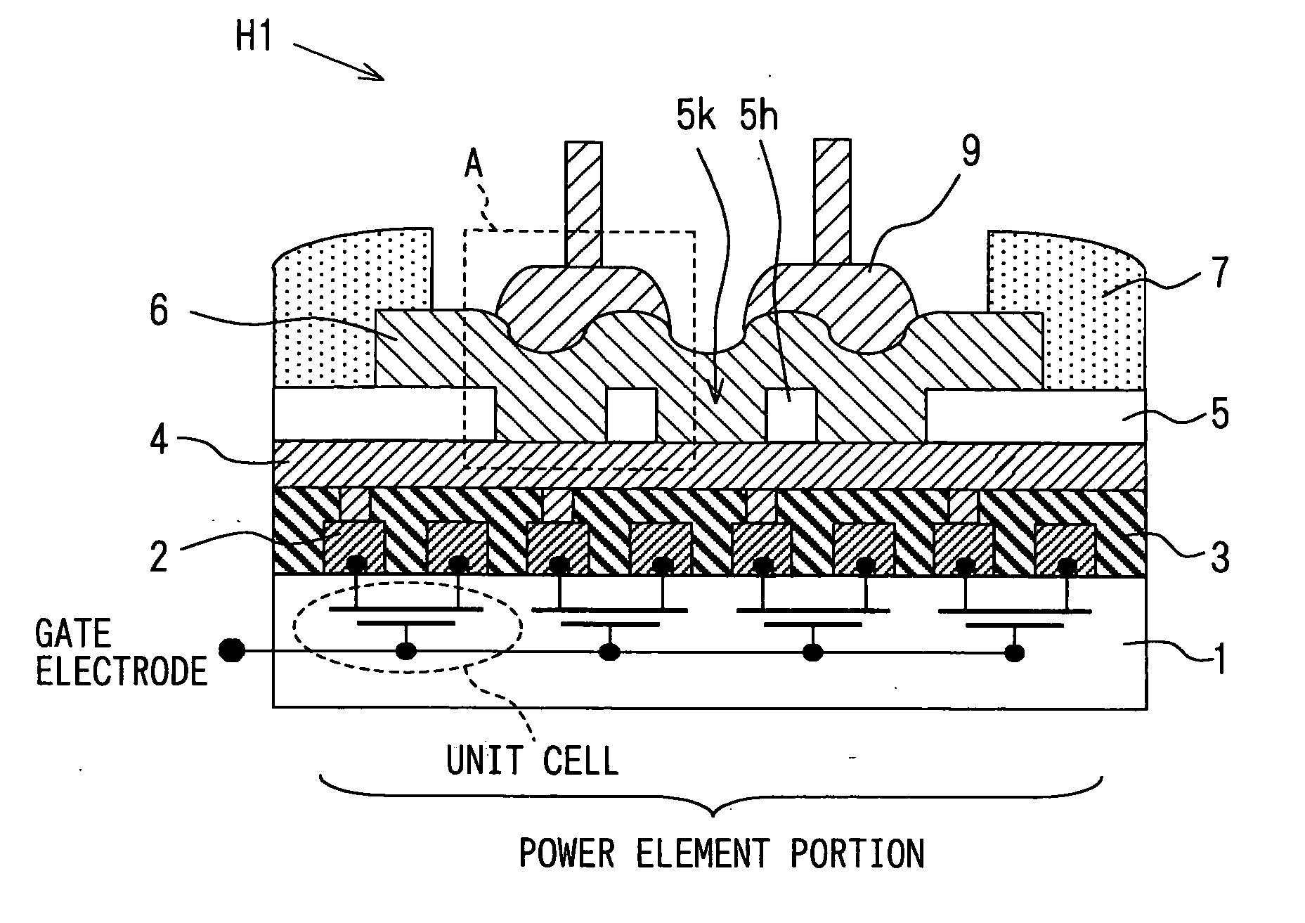
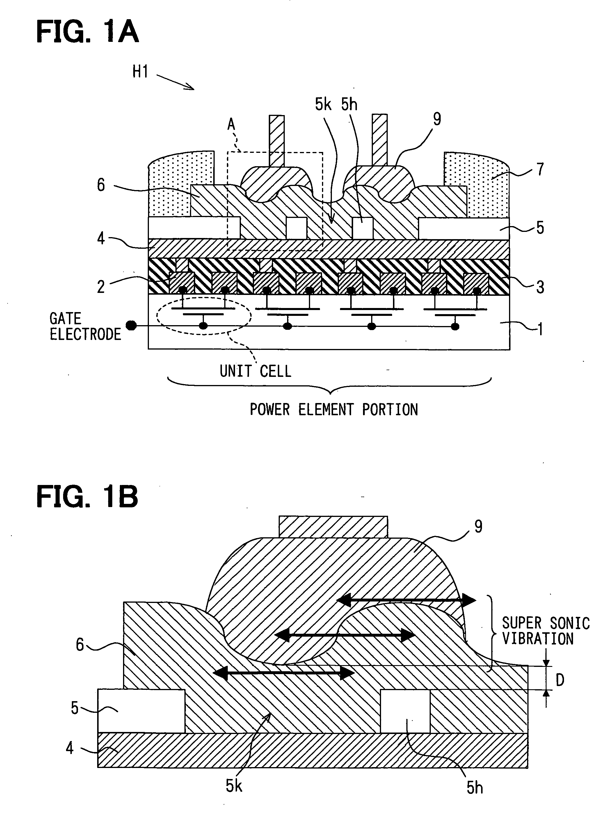
[0043]FIG. 1A is a schematic view showing a semiconductor device H1 according to a first embodiment of the present invention. Further, FIG. 1B is a partially enlarged view showing an A-part surrounded with a broken line in FIG. 1A, and the view explaining function of the first embodiment.

[0044] The semiconductor device H1 includes multiple power element unit cells such as a LDMOS (i.e., a Lateral Diffused MOS) unit cells formed in a silicon substrate 1. In the cells, gates, sources and drains are independently retrieved and connected in parallel. As shown in FIG. 1(a), a lead wire 2 is formed to connect to the source or the drain in each unit cell through a contact hole. The lead wire 2 connected to the source or the drain is connected to a collecting electrode 4 through a via hole formed in the interlayer insulation layer 3. The collecting electrode 4 is connected to the source or the drain in parallel. FIG. 1(a) schematically shows the collecting electrode 4 for connecting the le...

second embodiment

[0066]FIG. 8 is a schematic view showing a semiconductor device H2 according to a second embodiment of the present invention. In the semiconductor device H2 of this embodiment shown in FIG. 8, similar to the semiconductor device H1 according to the first embodiment, multiple power element unit cells are formed on the surface portion of the silicon substrate 1. Here, the construction disposed under the collecting electrode 4 in the semiconductor device H2 shown in FIG. 8 is similar to that of the semiconductor device H1 shown in FIG. 1(a); and therefore, the description of the construction is skipped.

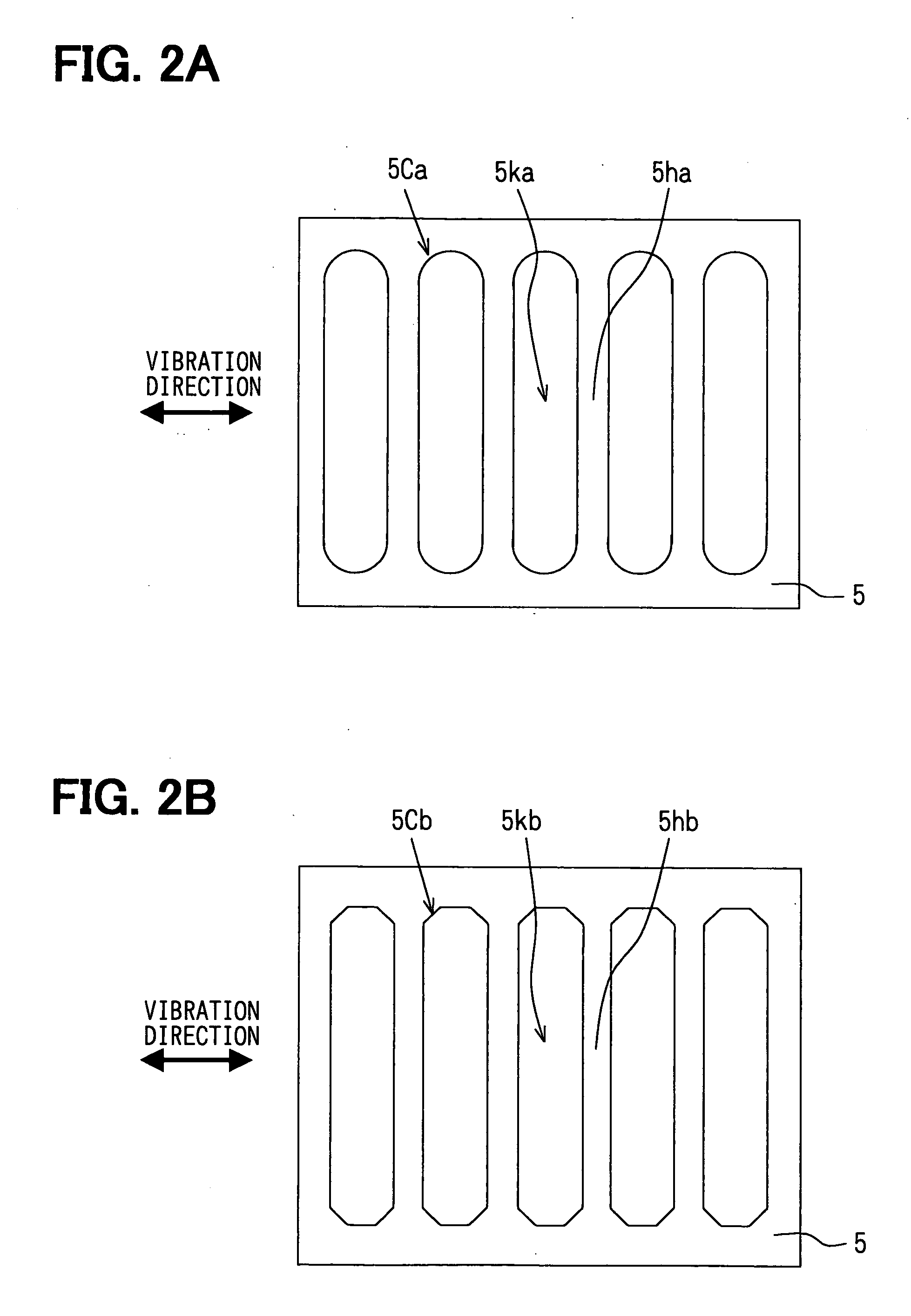
[0067] In the semiconductor device H2 shown in FIG. 8, the interlayer protection film 5 is formed on the collecting electrode 4 made of aluminum or aluminum alloy, similar to the semiconductor device Hi shown in FIG. 1(a). Further, multiple openings 5k are adjacently disposed in the interlayer protection film 5 so that the impact-absorbing beam 5h is formed of the interlayer protection ...

third embodiment

[0078]FIG. 10(a) is a schematic cross sectional view showing a semiconductor device H3 according to this embodiment. FIG. 10(b) is a partially enlarged view showing a B-portion surrounded with a broken line in FIG. 10(a), and the view explaining function and effect of this embodiment.

[0079] In the semiconductor device H3 shown in FIG. 10(a), similar to the semiconductor devices H1, H2 according to the first and the second embodiments, the power element unit cells are disposed on the surface portion of the silicon substrate 1. Here, in the semiconductor device H3 shown in FIG. 10(a), the construction disposed under the collecting electrode 4 is similar to that of the power element combined integration type semiconductor device Hi shown in FIG. 1(a); and therefore, the description of the construction is skipped.

[0080] In the semiconductor device H3 shown in FIG. 10(a), the interlayer protection film 50 is formed on the collecting electrode 4. The interlayer protection film 50, diffe...


PUM


Abstract

A semiconductor device includes: a plurality of power MOS cells on a semiconductor substrate; a plurality of lead wires connecting to a source and a drain of each power MOS cell through a contact hole; a plurality of collecting electrodes connecting in parallel with the lead wires through a via hole; an interlayer protection film on the collecting electrode; a thick film electrode connecting to the collecting electrode through the opening; and a terminal protection film having an opening for bonding connection. The openings are formed in the interlayer protection film such that a portion between the openings becomes a beam shape

Description

CROSS REFERENCE TO RELATED APPLICATIONS [0001] This application is based on Japanese Patent Applications No. 2004-328124 filed on Nov. 11, 2004, and No. 2005-298076 filed on October 12, the disclosures of which are incorporated herein by reference. FIELD OF THE INVENTION [0002] The present invention relates to an integration type semiconductor device and method for manufacturing the same. BACKGROUND OF THE INVENTION [0003] Conventionally, deformation or breakdown of a pad electrode or breakdown and the like of a region under the pad electrode becomes a problem. They are caused by bonding impact such as pressurization or supersonic vibration of a bonding connection, when an aluminum wire or a gold wire is bonded and connected to the pad electrode as an external output electrode of the semiconductor device. [0004] To improve failure of the pad electrode attributed to the bonding impact, as shown in FIG. 15, a first prior art (i.e., Japanese Laid-Open Patent Publication No. S63-161634)...

Claims


Application Information

Patent Timeline
IPC IPC(8): H01L23/52H01L21/3205H01L21/60H01L21/768H01L23/522
CPCH01L23/3114H01L23/53238H01L24/03H01L24/05H01L24/06H01L24/45H01L24/48H01L24/49H01L24/85H01L2224/02166H01L2224/04042H01L2224/05073H01L2224/05082H01L2224/05093H01L2224/05124H01L2224/05166H01L2224/05187H01L2224/05553H01L2224/05556H01L2224/05558H01L2224/05624H01L2224/45124H01L2224/45144H01L2224/4807H01L2224/48463H01L2224/48624H01L2224/48724H01L2224/49171H01L2224/85205H01L2924/01004H01L2924/01005H01L2924/01013H01L2924/01014H01L2924/01015H01L2924/01022H01L2924/01029H01L2924/01074H01L2924/01078H01L2924/01079H01L2924/01082H01L2924/04941H01L2924/05042H01L2924/10253H01L2924/13091H01L2924/14H01L2924/01006H01L2924/01033H01L2224/48453H01L2224/02125H01L2224/05557H01L2224/05554H01L2224/0603H01L2924/00014H01L2924/01007H01L2924/04953H01L2924/00H01L2924/00012H01L2224/05017H01L2224/45099H01L2924/00015
Inventor ITO, HIROYASU
Owner DENSO CORP
Why Eureka
Try Eureka