Patch antenna, array antenna, and mounting board having the same

a technology of array antennas and mounting boards, applied in the structural form of radiating elements, substantially flat resonant elements, resonance antennas, etc., can solve the problems of dielectric loss, ineffective method of increasing the gain of rectangular antennas, and more likely to affect the electric characteristics of dielectrics, etc., to achieve the effect of improving the antenna characteristics

Active Publication Date: 2006-05-11
SHINKO ELECTRIC IND CO LTD +1
View PDF3 Cites 17 Cited by
  • Summary
  • Abstract
  • Description
  • Claims
  • Application Information

AI Technical Summary

Benefits of technology

[0010] Accordingly, it is a general object of the present invention to provide a patch antenna and an array antenna in which the above-described disadvantages are eliminated.
[0011] A more specific object of the present invention is to provide a patch antenna and an array antenna that can improve antenna characteristics, and a mounting board having such an array antenna.
[0013] According to one embodiment of the present invention, it is possible to reduce the length of a feeding circuit up to an antenna part, that is, a radiation element, so that it is possible to reduce power loss.
[0015] According to one embodiment of the present invention, it is possible to improve antenna gain with the above-described configuration.
[0017] According to one embodiment of the present invention, it is possible to arrange radiation elements with a reduced pitch with the above-described configuration.
[0019] According to embodiments of the present invention, it is possible to achieve a patch antenna and an array antenna that can improve antenna characteristics, and a mounting board having such an array antenna.

Problems solved by technology

Further, since an extension circuit up to the antenna input part is increased in length, the antenna is more likely to be affected by the electric characteristics of a dielectric, such as dielectric loss.
However, considering interconnection line density, this method is not effective as means of increasing the gain of a rectangular antenna.

Method used


Image

  • Patch antenna, array antenna, and mounting board having the same
  • Patch antenna, array antenna, and mounting board having the same
  • Patch antenna, array antenna, and mounting board having the same

Examples


first embodiment

[0036] A description is given, with reference to FIGS. 2 and 3, of the present invention.

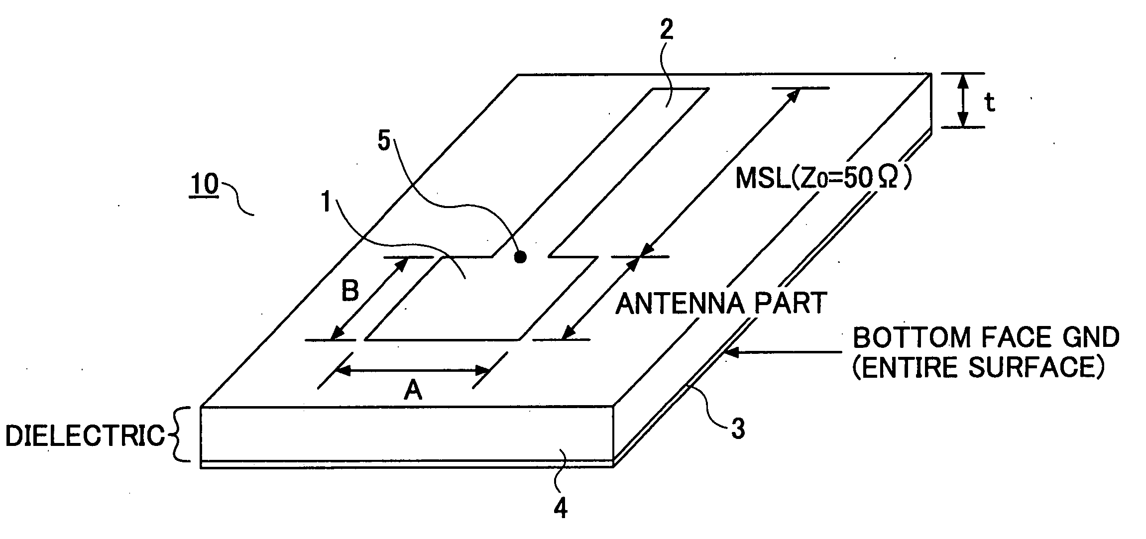
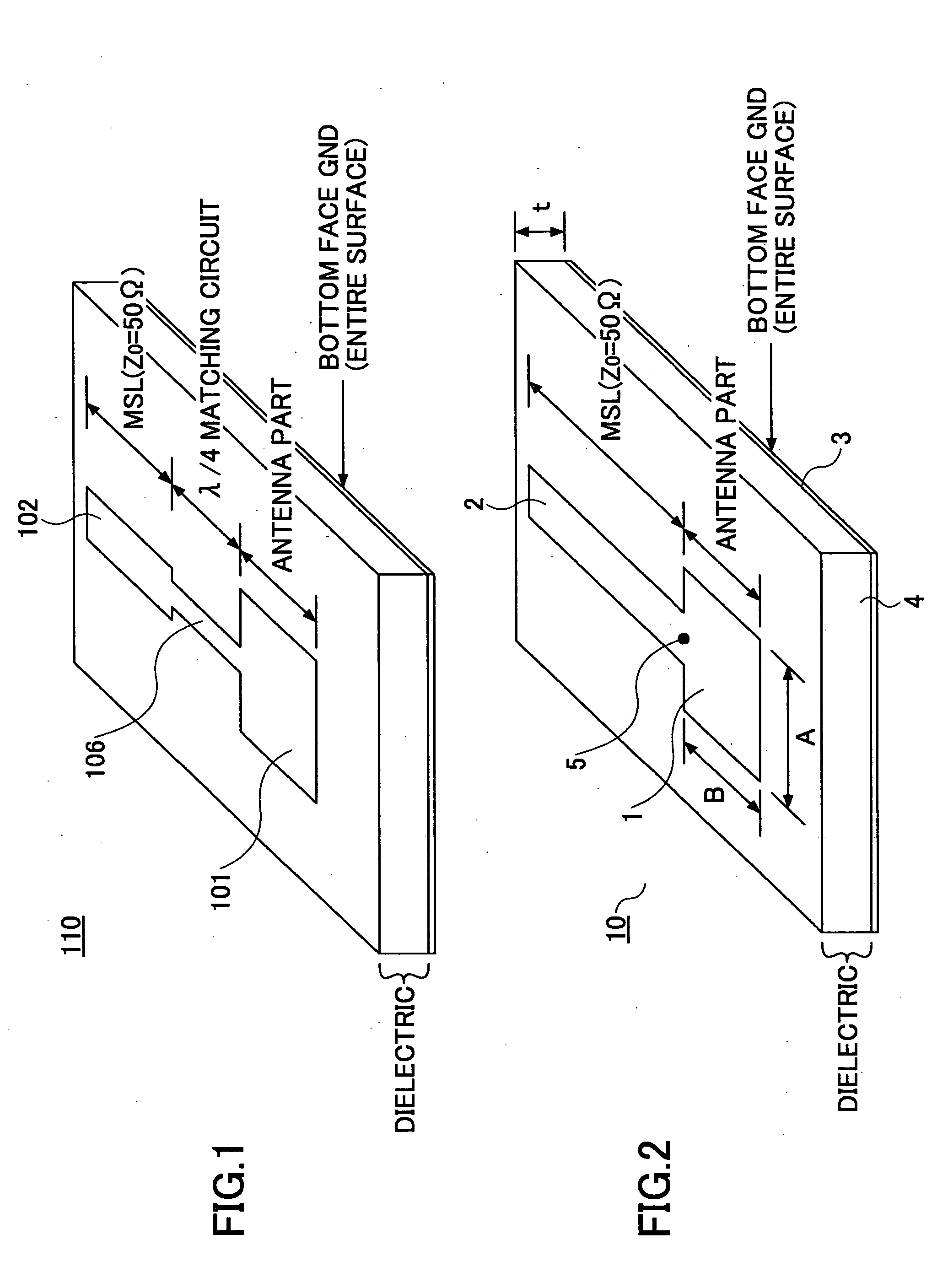
[0037]FIG. 2 is a perspective view of a patch antenna 10 according to the first embodiment. Referring to FIG. 2, the patch antenna 10 includes a dielectric substrate 4 of a thickness t and a dielectric constant εr and a substantially rectangular radiation element (patch) 1 of a conductive material formed on a first surface of the dielectric substrate 4. A ground (GND) layer 3 is formed on a second or bottom surface of the dielectric substrate 4 on the opposite side from the first surface. Two adjacent sides of the radiation element 1 are A and B in length, where A is greater than B (A>B). A feeding point 5 of the radiation element 1 is the end part of the radiation element 1 (antenna part) and is a predetermined part of an A-length side of the radiation element 1. A feeder line 2, for example, a microstrip line (MSL), is directly connected to the feeding point 5, so that feeding is performed.

[0...


PUM


Abstract

A patch antenna is disclosed that includes a dielectric substrate, a substantially rectangular radiation element formed of a conductive material on the dielectric substrate; and a feeder line connected to a feeding point for feeding to the radiation element. The feeding point has an impedance matching the impedance of the feeder line.

Description

BACKGROUND OF THE INVENTION [0001] 1. Field of the Invention [0002] The present invention relates generally to patch antennas, array antennas, and mounting boards having the same, and more particularly to a patch antenna and an array antenna used for GPS (Global Positioning System) and ETC (Electronic Toll Collection System), and a mounting board having the same. [0003] 2. Description of the Related Art [0004] In general, a patch antenna, which is a planar antenna, has a rectangular or circular shape. FIG. 1 is a perspective view of a patch antenna 110 of an MSL feeding type. As shown in FIG. 1, in the case of feeding to an antenna pattern by microstrip line (MSL) feeding, a matching circuit 106 that performs impedance matching is provided between an MSL 102 and an antenna part 101 since the MSL 102 has an impedance (Z0=50Ω) different from that of the input end of the antenna part 101. The matching circuit 106 is a circuit of a specific frequency (λ / 4, λ=wavelength) whose impedance ...

Claims


Application Information

Patent Timeline
Patent Type & Authority Applications(United States)
IPC IPC(8): H01Q1/38
CPCH01Q9/0407H01Q9/0442H01Q21/065
Inventor FUJII, TOMOHARUHIRACHI, YASUTAKENAKANO, HIROSHI
Owner SHINKO ELECTRIC IND CO LTD
Why Eureka
Try Eureka