Substrate cleaning method, substrate cleaning apparatus, susbtrate processing system, substrate cleaning program and storage medium

a cleaning method and substrate technology, applied in the direction of cleaning process and apparatus, cleaning process using liquids, chemistry apparatus and processes, etc., can solve the problems of substances adhering to the entire backside of the wafer, deteriorating the quality of the semiconductor device formed on the surface of the wafer, etc., to prevent the deterioration of the quality of the semiconductor device. , the effect of efficient removal

Inactive Publication Date: 2006-05-18
TOKYO ELECTRON LTD
View PDF5 Cites 12 Cited by
  • Summary
  • Abstract
  • Description
  • Claims
  • Application Information

AI Technical Summary

Benefits of technology

[0008] It is, therefore, an object of the present invention to provide a substrate cleaning method, a substrate cleaning apparatus, a substrate processing system, a substrate cleaning program and a storage medium, which are capable of completely removing deposits adhered to a backside of a substrate and also preventing quality deterioration of a semiconductor device formed on the substrate.
[0023] In accordance with the present invention, a two phase substance contacts the backside of the substrate; and a flow of the substance is generated near the backside of the substrate under a specified pressure. Since the two phase substance has two characteristics for the respective phases, deposits attached on the backside of the substrate can be efficiently detached due to the synergy effects of the two characteristics. Further, since the flow of the substance generated under the specified pressure becomes a viscous flow, the deposits detached from the backside of the substrate can be efficiently removed from a vicinity of the backside of the substrate. In this way, the deposits detached on the backside of the substrate can be completely removed, thereby preventing a semiconductor device formed on the substrate from being deteriorated in quality.
[0024] In case the two phase substance is a gas containing aerosol, the aerosol collides with the deposits attached on the backside of the substrate, so that the adhesion of the deposits becomes weak to be detached, and the gas carries the detached deposits. In this way, it is possible to surely remove the deposits detached on the backside of the substrate.
[0027] In case the supercritical substance contains an additive for dissolving the deposits adhered to the substrate, the additive completely surrounds the deposits due to the characteristics of the supercritical substance. Accordingly, the deposits can be efficiently dissolved.
[0029] Moreover, in accordance with the present invention, a high-energy light is irradiated on the backside of the substrate; and a flow of a substance is generated near the backside of the substrate under a specified pressure. The substrate on which the high-energy light has been irradiated is expanded, so that the deposits attached on the backside of the substrate can be efficiently detached due to a difference between the thermal expansion rate of the backside of the substrate and those of the deposits. Further, since the flow of the substance generated under the specified pressure becomes a viscous flow, the detached deposits are efficiently removed from a vicinity of the backside of the substrate. In this way, the deposits attached on the backside of the substrate can be completely removed, thereby preventing deterioration in quality of a semiconductor device formed on the substrate.

Problems solved by technology

Such particles are adhered to the wafer and thus deteriorate quality of a semiconductor device formed on a surface of the wafer.
However, in the aforementioned wet cleaning method, pure water or the like is ejected mostly toward a surface of the wafer.
Therefore, particles adhered to a backside of the wafer, i.e., foreign substances adhered to an entire backside of the wafer or bevel polymer adhered to a peripheral portion of the backside of the wafer, cannot be removed.
The wafer is kept afloat by the particles adhered to the backside of the wafer while it is mounted on the mounting table, so that, during a lithography process for exposing a photoresist coated on the wafer surface, a distance between the wafer and an exposure device does not coincide with a focal length of the exposure device and, therefore, a mask pattern cannot be precisely reproduced on the wafer surface.
Consequently, the quality of a semiconductor device formed on the corresponding wafer is deteriorated.
In case wafers undergone a predetermined plasma process are transferred in an airtight container such as a FOUP for holding a plurality of wafers in parallel, particles detached from a backside of a wafer held in an upper level in the FOUP may fall downward to be adhered to a surface of a wafer held in a lower level in the FOUP, thereby deteriorating the quality of a semiconductor device formed on the wafer held in the lower level in the FOUP.
Consequently, the quality of a semiconductor device formed on the wafer can be deteriorated.

Method used


Image

  • Substrate cleaning method, substrate cleaning apparatus, susbtrate processing system, substrate cleaning program and storage medium
  • Substrate cleaning method, substrate cleaning apparatus, susbtrate processing system, substrate cleaning program and storage medium
  • Substrate cleaning method, substrate cleaning apparatus, susbtrate processing system, substrate cleaning program and storage medium

Examples


Embodiment Construction

[0040] Hereinafter, preferred embodiments of the present invention will be described in detail with reference to the accompanying drawings.

[0041] First of all, a substrate cleaning apparatus and a substrate processing system in accordance with a first preferred embodiment of the present invention will be described.

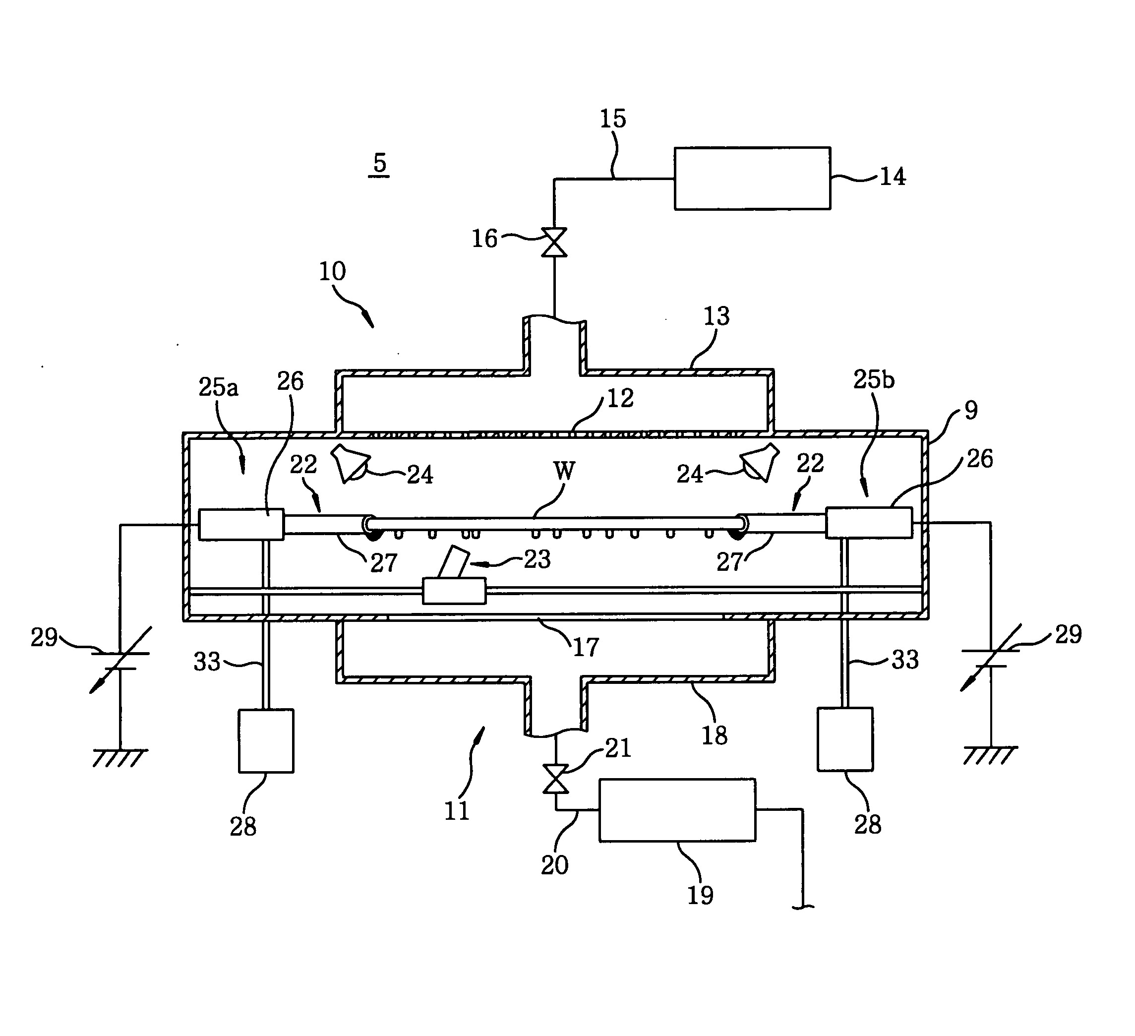
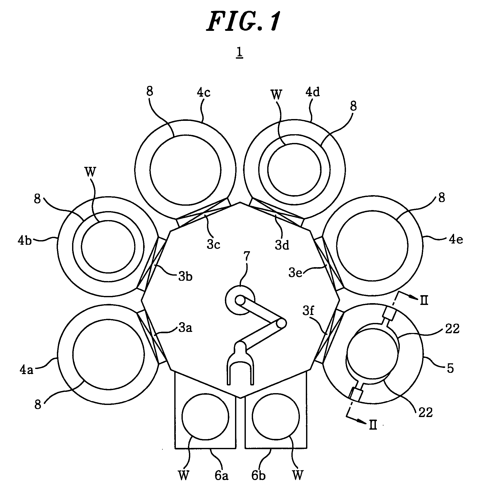
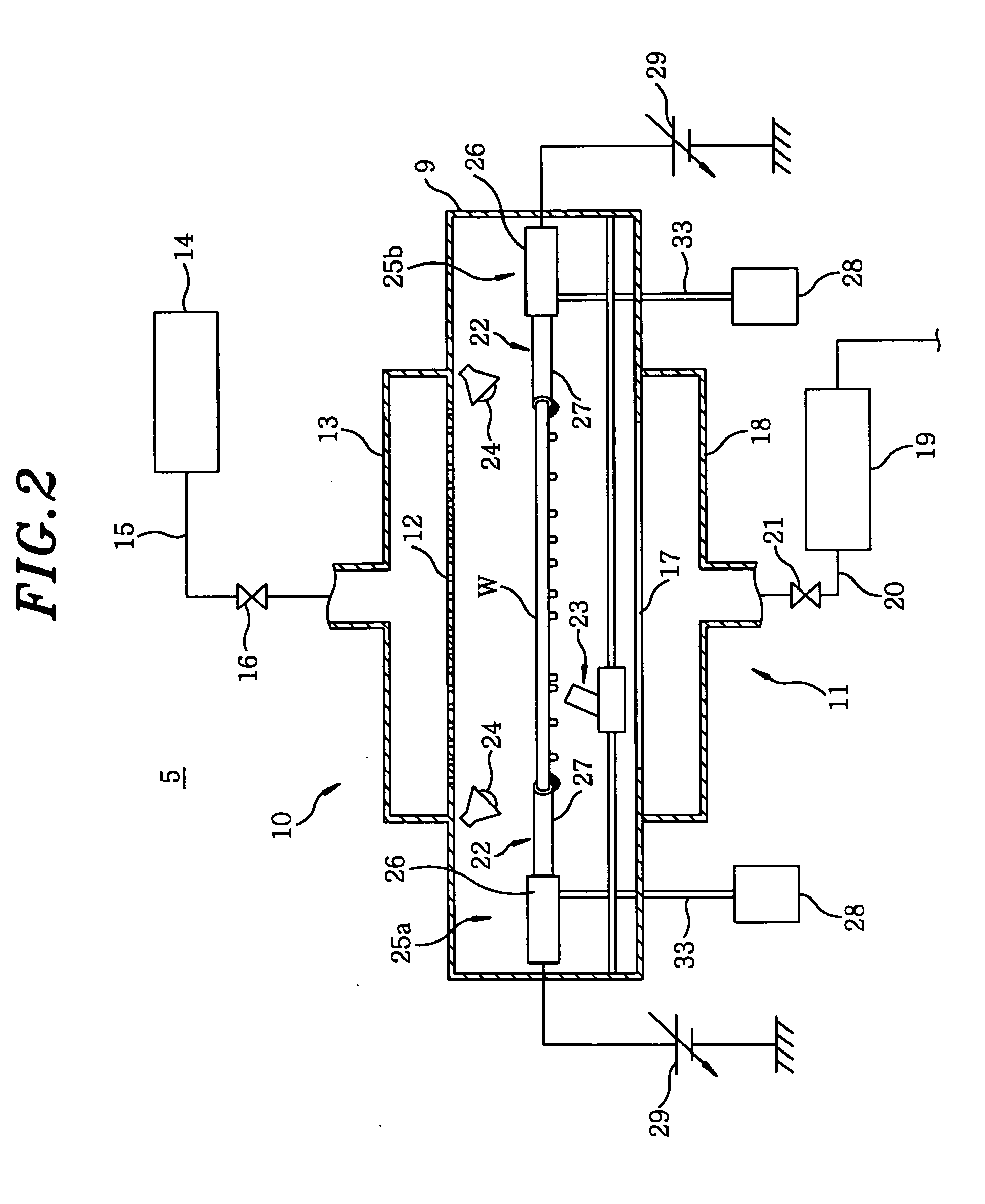
[0042]FIG. 1 is a top view schematically showing the substrate processing system in accordance with the first preferred embodiment.

[0043] Referring to FIG. 1, a cluster substrate processing system 1 includes: a polygonal transfer chamber 2; vacuum chambers 4a to 4e arranged along a periphery of the transfer chamber 2, the vacuum chambers serving as plasma processing chambers connected to sidewalls of the transfer chamber 2 via gate valves 3a to 3e; a single cleaning chamber (substrate cleaning apparatus) connected to a sidewall of the transfer chamber 2 via a gate valve 3f, same as the vacuum chambers 4a to 4e; and two cassette chambers 6a and 6b directly connected to s...


PUM

PropertyMeasurementUnit
pressureaaaaaaaaaa
atmospheric pressureaaaaaaaaaa
pressureaaaaaaaaaa

Abstract

In a substrate cleaning method for cleaning a backside of a substrate on a surface of which a predetermined processing is performed, a two phase substance contacts the backside of the substrate, and a flow of the substance is generated near the backside of the substrate under a specified pressure. The two phase substance is a gas containing aerosol or a supercritical substance, and the specified pressure is higher than or equal to 133 Pa (1 Torr). Further, in the substrate cleaning method, a high-energy light may be irradiated on the backside of the substrate.

Description

FIELD OF THE INVENTION [0001] The present invention relates to a substrate cleaning method, a substrate cleaning apparatus, a substrate processing system, a substrate cleaning program and a storage medium; and, more particularly, to a substrate cleaning method for removing deposits adhered to a backside of a substrate. BACKGROUND OF THE INVENTION [0002] In general, in a substrate processing apparatus for performing a processing on a semiconductor wafer (hereinafter, referred to as “wafer”) as a substrate, there are generated particles, e.g., fine fragments of aluminum, caused by a contact between the wafer and a mounting table for mounting thereon the wafer, reaction products, e.g., fluorocarbon-based polymer, caused by a reaction of a processing gas or the like. Such particles are adhered to the wafer and thus deteriorate quality of a semiconductor device formed on a surface of the wafer. [0003] As for a method for removing particles adhered to a wafer, there has been known a wet c...

Claims


Application Information

Patent Timeline
Patent Type & Authority Applications(United States)
IPC IPC(8): B08B3/00B08B3/12
CPCB08B7/0021B08B7/0035B08B7/0042H01L21/0209H01L21/02101H01L21/67028H01L21/67034Y10S134/902
Inventor MORIYA, TSUYOSHI
Owner TOKYO ELECTRON LTD
Why Eureka
Try Eureka