Semiconductor fabrication device heater and heating device equipped with the same

a technology of semiconductor fabrication and heating device, which is applied in the direction of ohmic-resistance heating, ohmic-resistance heating details, electrical apparatus, etc., can solve the problems of difficult to effectively form fine circuit patterns using photolithography, and achieve the effect of reducing the influence of environmental variations, quick cooling, and reducing the temperatur

Inactive Publication Date: 2006-05-18
WEST VIRGINIA UNIVERSITY +1
View PDF13 Cites 52 Cited by
  • Summary
  • Abstract
  • Description
  • Claims
  • Application Information

AI Technical Summary

Benefits of technology

[0013] After extensive research directed at overcoming these problems, the present inventors determined that temperature distribution in the heater can be improved compared with the conventional technology if the material for all or part of the base of the heater has a heat capacity per unit volume of at least 2.0 J / K·cm3 and a thermal conductivity of at least 50 W / mK.

Problems solved by technology

However, this does not provide improved throughput.
While controlling uniformity of temperature during the transitional state, e.g., 30 seconds after mounting the object to be heated on the heater, is extremely difficult, increasing throughput requires quickly increasing the temperature and quickly stabilizing temperature variations once a wafer is mounted on and temperature is reduced for the heater used in the PEB step and the PAB step.
This makes it difficult to form fine circuit patterns effectively using photolithography.

Method used


Image

  • Semiconductor fabrication device heater and heating device equipped with the same
  • Semiconductor fabrication device heater and heating device equipped with the same

Examples


first embodiment

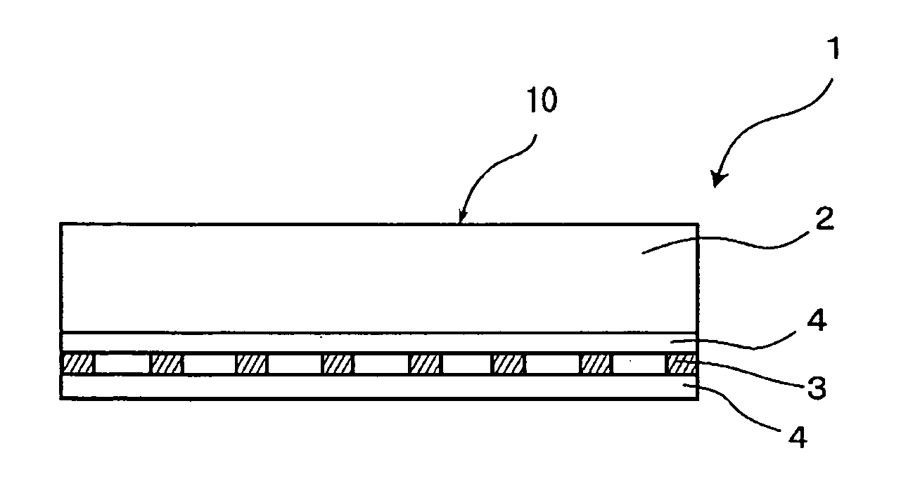
[0124] As shown in FIG. 1, a stainless steel resistance heating body 3 having a thickness of 50 microns and a diameter of 330 mm and in which a heater circuit is formed from a single zone is interposed between two polyimide plates (thickness 150 microns) serving as insulators 4. A copper plate 2 having a thickness of 15 mm and a diameter of 330 mm is attached, resulting in a heating body 1. The copper plate is nickel-plated.

[0125] This heating body was placed in a stainless steel container. The heating body was heated to 130 deg C. and a room-temperature (25 deg C.) wafer thermometer having a diameter of 300 mm was mounted on a heating surface 10. The temperature on the wafer thermometer was measured at 30 seconds after mounting, 60 seconds after mounting, and 5 minutes. The differences between the maximum measured temperature and the minimum measured temperature are shown in Table 1. The table also shows the heat capacity and the thermal conductivity of the copper plate used as th...

second embodiment

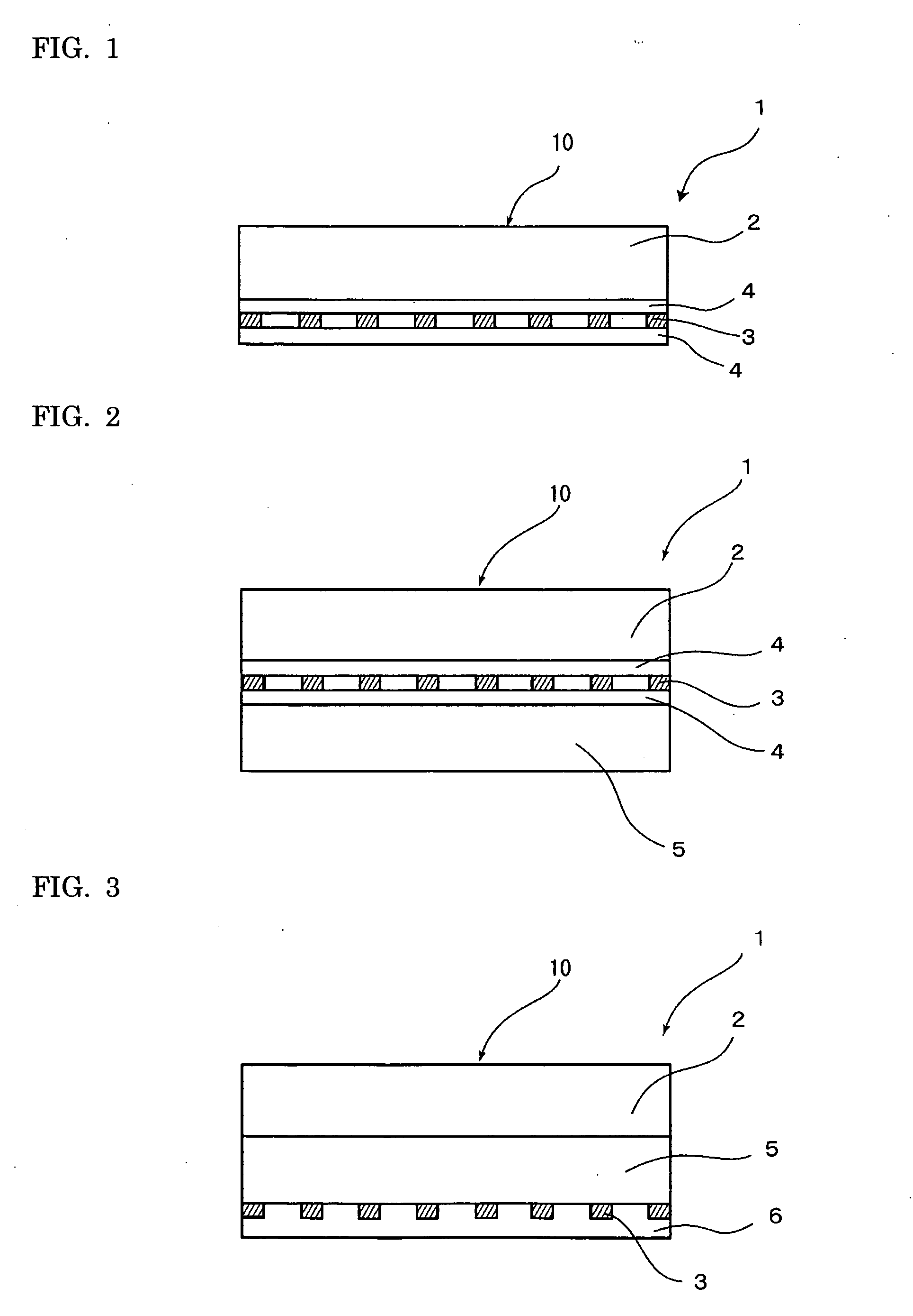
[0126] As shown in FIG. 2, a stainless steel resistance heating body 3 having a thickness of 50 microns and a diameter of 330 mm was interposed between two polyimide plates 4 as in the first embodiment, and this was then placed between a base 5 and a base 2 having a diameter of 330 mm, resulting in a heating body 1. The thickness of the base 2 was 4.5 mm and the thickness of the base 5 was 10.5 mm. The materials used for the base 2 and the base 5 are as shown in Table 2. The copper plates were nickel-plated. These heating bodies were attached in a stainless steel container and, as in the first embodiment, a wafer thermometer was mounted on the heating surface and temperature ranges were measured after 30 seconds, 60 seconds, and 5 minutes. The results, along with the heat capacity and the thermal conductivity of the bases are shown in Table 2.

TABLE 2TemperatureHeatThermalranges (° C.)capacityconductivity60Base 2Base 5(J / Kcm3)(W / mK)30 secsec5 minNiNi3.9940.150.090.08FeFe3.4840.170....

third embodiment

[0127] A heating body was prepared and temperature ranges were measured with a wafer thermometer as in the second embodiment except that, as shown in Table 3, metal and ceramic composite bodies were used as the material for the base 2 and the base 5. The results are shown in Table 3. In the table, Si-70SiC, for example, indicates a composite material of Si and SiC with an SiC content of 70 percent by weight.

TABLE 3ThermalHeat capacityconductivityTemperature ranges (° C.)Base 2Base 5(J / Kcm3)(W / mK)30 sec60 sec5 minSi—70SiCSi—70SiC3.01720.130.100.07Al—30SiCAl—30SiC2.31500.170.130.10Al—AlNAl—AlN2.81760.130.100.07


PUM

PropertyMeasurementUnit
distanceaaaaaaaaaa
flatnessaaaaaaaaaa
temperatureaaaaaaaaaa

Abstract

A heating body and a device equipped with the same provide greater uniformity in temperature distribution between the start of heating and the end of cooling. A semiconductor fabrication device heating body includes a base having a heating surface upon which an object is mounted or positioned at a fixed distance away and is heated, and a resistance heating body. All or part of the base of the heating body has a thermal capacity per unit volume of at least 2.0 J / K·cm3 and a thermal conductivity of at least 50 W / mK.

Description

BACKGROUND OF THE INVENTION [0001] 1. Field of the Invention [0002] The present invention relates to a heater for mounting and heating an object to be heated and a device equipped with the same. More specifically, the present invention relates to a heater and a heating device equipped with the same that is suitable for semiconductor fabrication devices and is used in particular to heat semiconductor wafers. [0003] 2. Description of the Background Art [0004] Conventionally, in semiconductor fabrication, a semiconductor substrate (wafer) undergoes various operations such as film formation and etching. Semiconductor fabrication devices that perform these operations on semiconductor substrates use a heater to support and heat a semiconductor substrate. [0005] For example, in a photolithography step, a resist film pattern is formed on the wafer. In this step, after the wafer is washed, dried with heat, and cooled, a resist film is applied to the wafer surface, the wafer is mounted on a h...

Claims


Application Information

Patent Timeline
Patent Type & Authority Applications(United States)
IPC IPC(8): H05B3/68
CPCH01L21/67103H05B3/12H05B3/262H01L21/67109
Inventor KUIBIRA, AKIRAMIKUMO, AKIRANATSUHARA, MASUHIRONAKATA, HIROHIKO
Owner WEST VIRGINIA UNIVERSITY
Why Eureka
Try Eureka