Process for producing ptc element/metal lead element connecting structure and ptc element for use in the process
- Summary
- Abstract
- Description
- Claims
- Application Information
AI Technical Summary
Benefits of technology
Problems solved by technology
Method used
Image
Examples
example 1
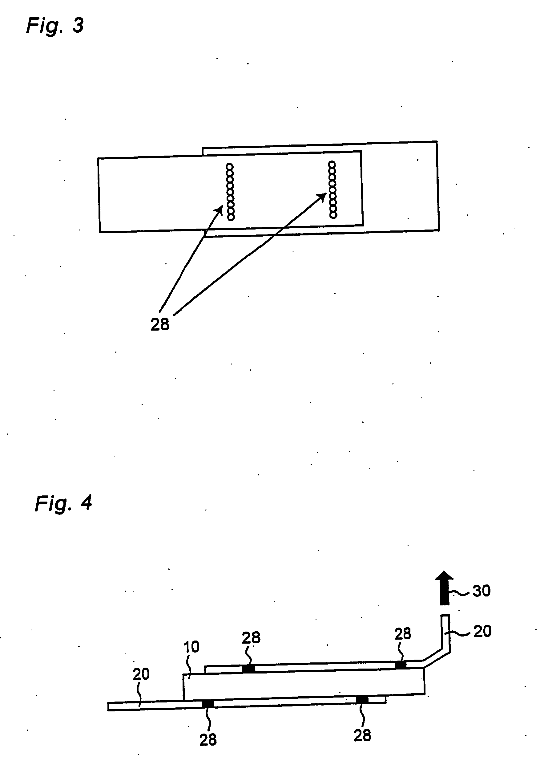
[0068] A polymer PTC device (a chip for VTP210 (trade name), manufactured by Tyco Electronics) was used, which was obtained by thermocompression-bonding copper foils (thickness: 60 μm) plated with nickel layers (thickness: 20 μm) to both main surfaces of a polyethylene PTC element with a size of 5 mm (width)×12 mm (length)×0.25 mm (thickness) (LB832 (trade name) manufactured by MILENNIUM CHEMICAL, U.S.A.) as the polymer PTC element. As the metal lead element, a nickel lead element with a size of 4 mm (width)×16 mm (length)×1.25 mm (thickness) was used. A YAG laser beam with an output of 1.8 W per pulse was applied to the nickel lead element and the PTC device for 0.7 sec. to carry out the pulse seam welding. In this regard, nine pulses of laser beam application constitutes one line, and two lines of welding were carried out. FIG. 3 shows an example of two lines of welding of the metal lead element to the PTC device, wherein nine pulse seams constitute one line.
[0069] Strength of th...
PUM
 Abstract
Description
Claims
Application Information

