Frequency selection using capacitance multiplication

Inactive Publication Date: 2006-05-18
AVAGO TECH INT SALES PTE LTD
View PDF3 Cites 3 Cited by
  • Summary
  • Abstract
  • Description
  • Claims
  • Application Information

AI Technical Summary

Problems solved by technology

Integrated Circuit (IC) designers are often challenged to reduce costs.
Many analog blocks require implementation of capacitors, which typically occupy larger areas of space in the IC as compared to other elements.
However, a limited range of linear operation of MOS capacitors makes the task of matching capacitance between two separate MOS capacitors inanely difficult, in large part because conventional MOS capacitors have a limited range of linear operation and frequency.
Thus, post-manufacture adjustment of the capacitance of MOS capacitor devices becomes very limited in a range that's linear.
As a result, MOS capacitors have limited use in a variable capacitance design, without complicated accommodation for the non-linearity of the capacitance due to the limited range of linear operation and frequency of such devices.
Therefore, preferably matched MOS capacitors are manufactured to have capacitances within very tight tolerances of one another, adding further to manufacturing costs.
Also, device drop out will increase, meaning that more devices will be discarded because of too-large a mis-match in capacitance between the MOS capacitors that are intended to be matched.
Higher device drop outs adds again to the cost of manufacture.
Moreover, for large values of LC, large capacitors are required.
To some extent, the larger the necessary capacitance, the larger the device must be, again occupying valuable space and working against the need for smaller and more efficient devices, and even limiting the miniaturization thereof.

Method used


Image

  • Frequency selection using capacitance multiplication
  • Frequency selection using capacitance multiplication
  • Frequency selection using capacitance multiplication

Examples


Embodiment Construction

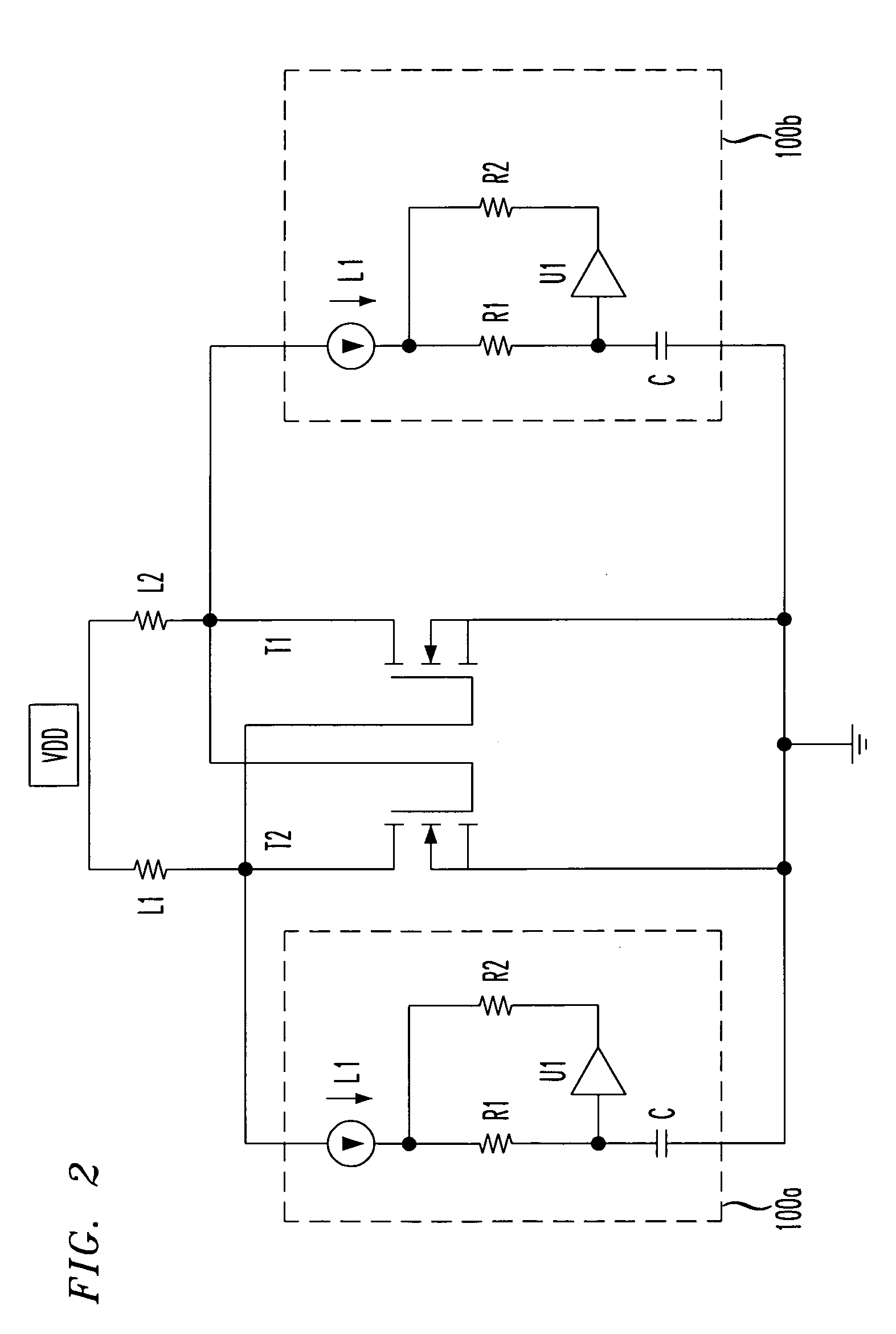
[0025] In accordance with the principles of the present invention, a capacitance multiplier circuit provides large values of capacitance using small valued capacitors. Moreover, such a VCO including a capacitance multiplier circuit uses less silicon area than otherwise conventional variable frequency devices.

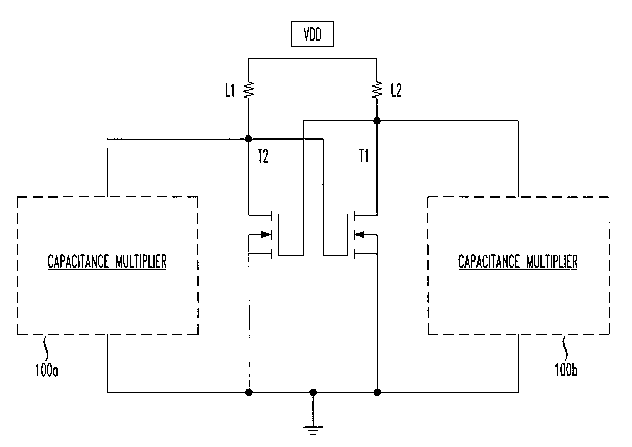
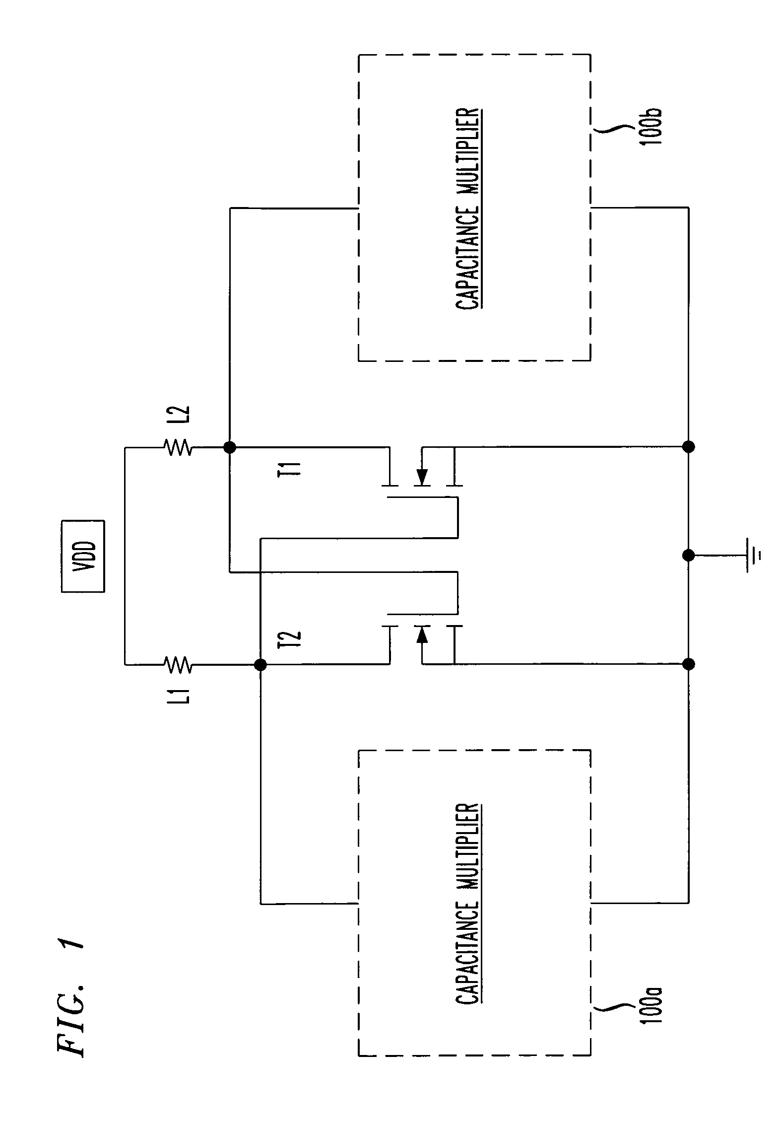
[0026]FIG. 1 shows two matched MOS capacitor devices, each being capacitance multiplied by a respective capacitance multiplier, in accordance with the principles of the present invention.

[0027] In particular, as shown in FIG. 1, cross-coupled MOS devices T1, T2 are matched to have identical characteristics. An inductor L1 is in series with a first MOS transistor device T2 between power and ground, and a second inductor L2 is in series with a second MOS transistor device T1 between power and ground.

[0028] Importantly, in the circuit of FIG. 1, capacitance multipliers 100a and 100b (collectively referred to by the reference designator 100) are implemented to both provide adjust...


PUM


Abstract

A variable capacitance circuit on an integrated circuit comprises a MOS transistor, and a capacitance multiplier connected to one end of a channel of the MOS device. A MOS device is formed in series with an inductance, and a capacitance multiplier is formed to be connected to a node between the MOS device and the inductance.

Description

BACKGROUND OF THE INVENTION [0001] 1. Field of the Invention [0002] This invention relates to integrated circuits. More particularly, it relates to an integrated circuit having variable frequency selection. [0003] 2. Background of Related Art [0004] Integrated Circuit (IC) designers are often challenged to reduce costs. At the same time, designers are challenged to increase performance of various circuit blocks on their ICs, and of course to decrease size of the IC. [0005] Analog circuit designers in particular are faced with achieving better circuit performance in standard digital complementary metal-oxide semiconductor (CMOS) processes. Many analog blocks require implementation of capacitors, which typically occupy larger areas of space in the IC as compared to other elements. It is known that a capacitor, or perhaps more correctly that capacitance, may be formed on an IC using a metal-oxide semiconductor (MOS) process. A MOS capacitor is, in reality, a MOS transistor connected in...

Claims


Application Information

Patent Timeline
IPC IPC(8): H03K5/00
CPCH03B2201/025H03H11/405H03J2200/10H03B5/1228H03B5/1212H03B5/1237H03H11/483
Inventor AZIMI, KOUROSGABARA, THADDEUS
Owner AVAGO TECH INT SALES PTE LTD
Why Eureka
Try Eureka