Microlens manufacturing method
- Summary
- Abstract
- Description
- Claims
- Application Information
AI Technical Summary
Benefits of technology
Problems solved by technology
Method used
Image

Examples
first preferred embodiment
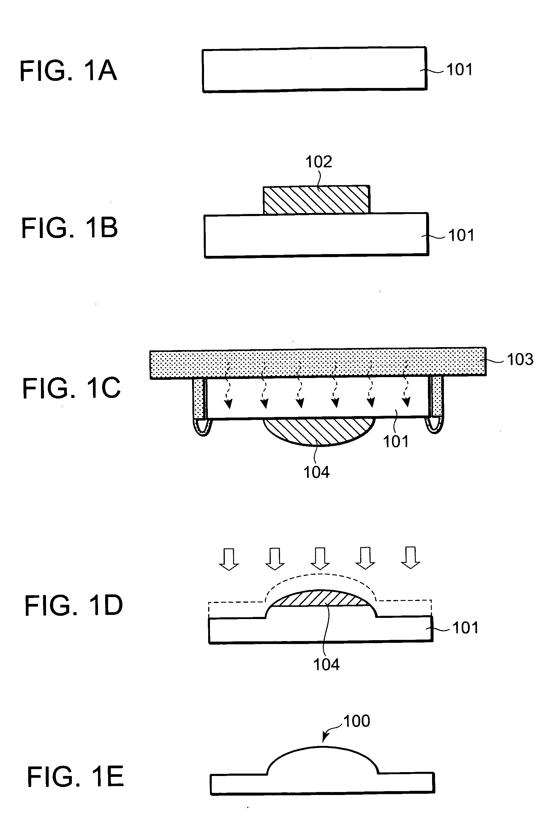
[0017]FIGS. 1A through 1E are process sectional views showing a method for manufacturing a microlens, according to a first embodiment of the present invention.
[0018] As shown in FIG. 1A, a semiconductor substrate 101 for fabricating the microlens is first prepared. The semiconductor substrate 101 is a silicon substrate, for example.
[0019] Next, as shown in FIG. 1B, a resist is applied onto the semiconductor substrate 101 to form a resist pattern 102 shaped in the form of a substantially circular cylinder by using the known photolithography. Now, the applied thickness of resist is suitably set according to the size of a formed lens. When, however, a lens having a diameter having approximately 100 μm, for example is formed, the applied thickness of resist may be set to approximately 10 to 50 μm.
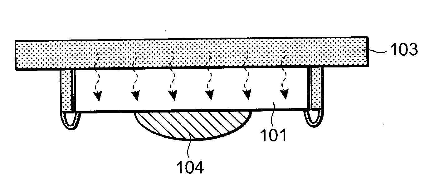
[0020] Next, as shown in FIG. 1C, the semiconductor substrate 101 formed with the resist pattern 102 is placed on a hot plate 103 with being turned upside down, i.e., a surface thereof with ...
second preferred embodiment
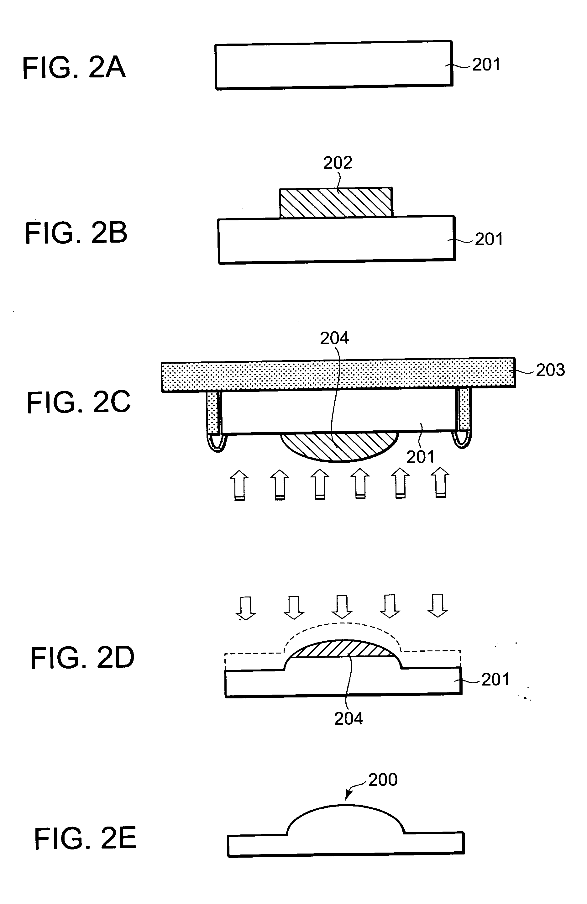
[0025]FIGS. 2A through 2E are process sectional views showing a method for manufacturing a microlens, according to a second embodiment of the present invention.
[0026] As shown in FIG. 2A, a semiconductor substrate 201 for fabricating the microlens is first prepared. The semiconductor substrate 201 is a silicon substrate, for example.
[0027] Next, as shown in FIG. 2B, a resist is applied onto the semiconductor substrate 201 to form a resist pattern 202 approximately cylindrical in form by using the known photolithography. Now, the applied thickness of resist is suitably set according to the size of a formed lens. When, however, a lens having a diameter of approximately 100 μm, for example is formed, the applied thickness of resist may be set to approximately 10 to 50 μm.
[0028] Next, as shown in FIG. 2C, the semiconductor substrate 201 formed with the resist pattern 202 is fixed to a predetermined support device 203 with being turned upside down, i.e., a surface thereof with the res...
PUM
 Abstract
Description
Claims
Application Information
 - Generate Ideas
- Intellectual Property
- Life Sciences
- Materials
- Tech Scout
- Unparalleled Data Quality
- Higher Quality Content
- 60% Fewer Hallucinations
Browse by: Latest US Patents, China's latest patents, Technical Efficacy Thesaurus, Application Domain, Technology Topic, Popular Technical Reports.
© 2025 PatSnap. All rights reserved.Legal|Privacy policy|Modern Slavery Act Transparency Statement|Sitemap|About US| Contact US: help@patsnap.com