
Semiconductor device, method and apparatus for fabricating the same

Active Publication Date: 2006-05-25
DENSO CORP
View PDF5 Cites 40 Cited by
  • Summary
  • Abstract
  • Description
  • Claims
  • Application Information

AI Technical Summary

Benefits of technology

[0041] In the case where a plurality of the semiconductor elements (10, 11) are included, the probable difference in thickness between them often makes it necessary to machine the main surfaces (20a, 30a) in order to make radiation surfaces parallel to each other. The aspect of the invention has the more advantageous effects for the semiconductor device having a plurality of the semiconductor elements.
[0042] According to a second aspect of the invention, there is provided a method of fabricating a semiconductor device, wherein a work including at least one semiconductor element (10, 11) and at least one radiator plate (20, 30) which is thermally connected to the semiconductor element (10, 11) is arranged in a die (200) so as to be covered and sealed with a molded resin (80), comprising the steps of: arranging a heat-resistant and flexible sheet (300) larger than an outer main surface (20a, 30a) of the radiator plate (20, 30) on a portion of the die (200) facing the main surface (20a, 30a); and pressing the main surface (20a, 30a) against the sheet (300) so as to seal the work with the molded resin (80) while covering the sheet on at least a part of the side surface (20b, 30b) adjoining the main surface (20a, 30a) of the radiator plate.
[0043] In this way, the main surfaces (20a, 30a) i.e. the radiation surfaces are pressed against the heat-resistant, flexible sheet (300) larger than the main surfaces (20a, 30a), and therefore the sheet (300) is deformed so that the main surfaces (20a, 30a) of the radiator plates (20, 30) sink into the sheet (300).
[0044] As a result, at least the neighborhood of the outer peripheral edge of the main surfaces (20a, 30a) of the radiator plates (20, 30), i.e. the neighborhood of the boundaries (20c, 30c) between the side surfaces (20b, 30b) and the main surfaces (20a, 30a) is covered in close contact with the deformed sheet (300).
[0045] Under this condition, the assembly is sealed with the molded resin (80) thereby making it possible to fabricate the semiconductor device according to the first aspect appropriately. In other words, according to the second aspect of the invention, there is provided a method of fabricating the semiconductor device according to the first aspect of the invention in an appropriate manner.
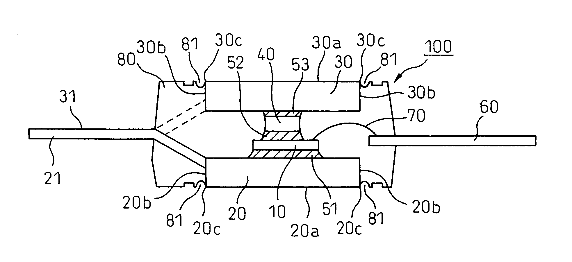
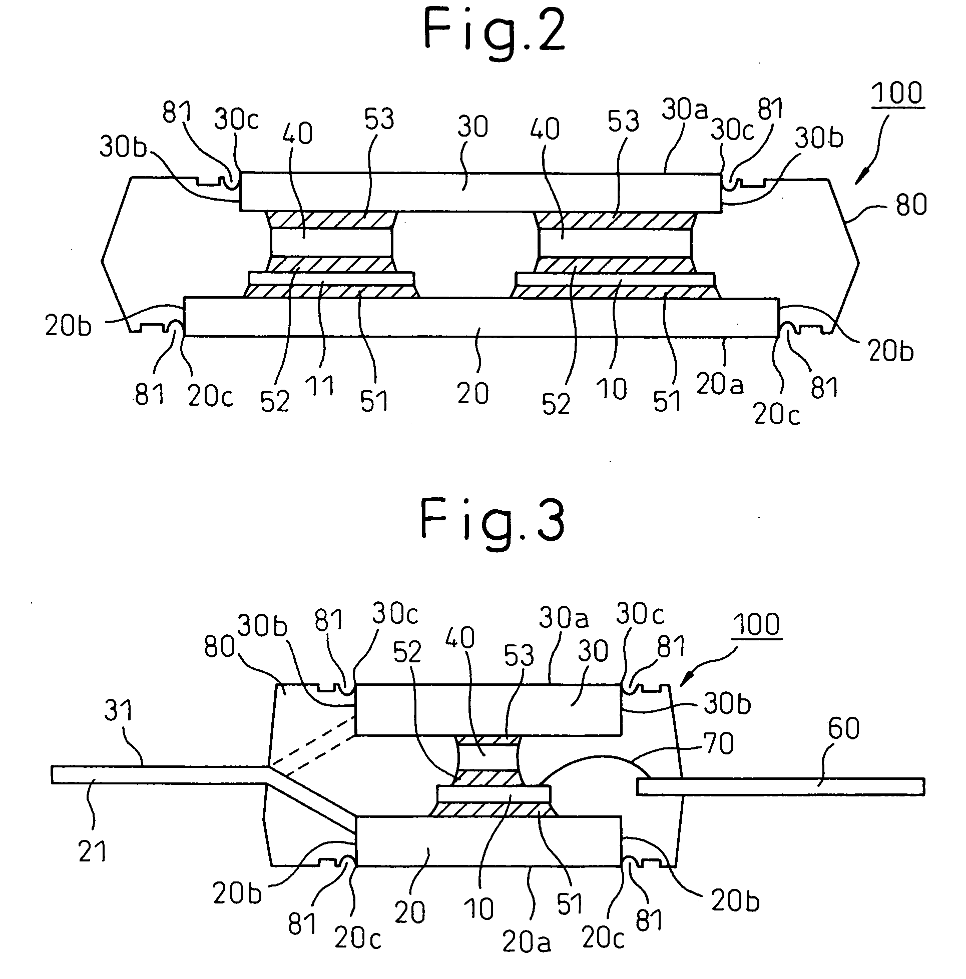
[0046] The semiconductor device obtained according to the second aspect has the semiconductor element (10, 11) connected to the radiator plates (20, 30) and sealed by the molded resin (80) and the radiation surfaces are so appropriately exposed. Therefore, the outer main surfaces (20a, 30a) i.e. the radiation surfaces of the radiator plates (20, 30) can be machined while reducing the consumption of the machining tool, thereby improving the life of the machining tool considerably.

Problems solved by technology

Therefore, it is difficult to hold the two radiation surfaces parallel to each other.
In this case, however, a poor parallelism between the radiation surfaces of the radiator plates would lead to a gap and an insufficient contact between each radiation surface and the corresponding cooling member, thereby often deteriorating the heat radiation efficiency.
This is due to the often irregular thickness of the semiconductor elements which makes it difficult to maintain the parallelism between the radiation surfaces.
When the radiation surfaces 20a, 30a are cut or ground with a machining member such as a cutting tool or a grinding stone, therefore, the risk of the machining member cutting the very hard molded resin 80 together with the radiator plates 20, 30 results in a very great consumption of the machining member.
Thus, the life of the machining member is considerably shortened and the cost of machining the radiation surfaces becomes higher.
The shot blasting is not undesirable, however, because of the need of the cleaning and drying processes after machining and a higher cost of materials such as abrasives.
The aforementioned problem of the great consumption and the shorter life of the machining member for cutting or grinding the radiation surfaces is not limited to the semiconductor device in which the two surfaces of the semiconductor element are sandwiched by a pair of radiator plates and the assembly is sealed with the molded resin while exposing the heat radiation surface of each radiator plate.

Method used


Image

  • Semiconductor device, method and apparatus for fabricating the same
  • Semiconductor device, method and apparatus for fabricating the same
  • Semiconductor device, method and apparatus for fabricating the same

Examples


Embodiment Construction

[0071] Embodiments of the invention are described below with reference to the drawings. In the drawings, the identical or equivalent parts are designated by the same reference numerals, respectively, to simplify the explanation.

[0072]FIG. 1 is a plan view schematically showing a semiconductor device 100 according to an embodiment of the invention. FIG. 2 is a diagram schematically showing a sectional structure taken in one-dot chain II-II in FIG. 1, and FIG. 3 a diagram schematically showing a sectional structure taken in one-dot chain III-III in FIG. 1.

[0073] In FIG. 1, a molded resin 80 is shown only as an outline thereof, and the planar arrangement of the parts located in the molded resin 80 is shown in a perspective drawing.

[0074] As shown in FIGS. 1 to 3, the semiconductor device 100 according to this embodiment includes semiconductor chips 10, 11 constituting semiconductor elements, and a pair of heat sinks 20, 30 formed with a pair of radiator plates arranged on the two su...


PUM


Abstract

A semiconductor device has at least one semiconductor element, at least one radiator plate thermally connected with said semiconductor element, and a molded resin covering and sealing said semiconductor device and said radiator, wherein an outer main surface of the radiator plate and at least a part of the side surface adjoining the outer main surface are exposed from the molded resin.

Description

BACKGROUND OF THE INVENTION [0001] 1. Field of the Invention [0002] This invention relates to a semiconductor device formed by sealing at least a semiconductor element thermally connected to a radiator plate with a molded resin, a method of fabricating the semiconductor device and an apparatus for fabricating the semiconductor device, or in particular to a semiconductor device formed by sealing at least a semiconductor element sandwiched between a pair of radiator plates with a molded resin, a method of fabricating the semiconductor device and an apparatus for fabricating the semiconductor device. [0003] 2. Description of the Related Art [0004]FIG. 7 is a schematic diagram showing a sectional structure of an ordinary resin molded semiconductor device. [0005] Generally, in the semiconductor of this type, as shown in FIG. 7, the two surfaces of a semiconductor element 10 are sandwiched by radiator plates 20, 30 and the resulting assembly is sealed with a molded resin 80 so as to expos...

Claims


Application Information

Patent Timeline
IPC IPC(8): H01L23/28
CPCH01L21/565H01L23/4334H01L2924/1305H01L2924/1301H01L2924/1815H01L2924/01019H01L2924/01006H01L2924/01005H01L24/49H01L24/48H01L2924/13055H01L2924/01082H01L2924/01079H01L2924/0105H01L2924/01033H01L2924/01029H01L2924/01013H01L2924/01004H01L2924/01002H01L2224/73265H01L2224/73215H01L2224/49171H01L2224/48472H01L2224/48247H01L24/32H01L24/33H01L25/072H01L2224/32245H01L2224/48091H01L2924/00014H01L2924/00H01L2924/00012H01L2924/181H01L24/73H01L2224/45124H01L2224/45144H01L2224/33H01L24/45H01L2224/2612H01L2224/45015H01L2924/207
Inventor NAKAZAWA, SHUSAKUONOUE, TSUTOMUMIZUNO, HIROAKINASU, HIDEHISA
Owner DENSO CORP
Features
  • Generate Ideas
  • Intellectual Property
  • Life Sciences
  • Materials
  • Tech Scout
  • Unparalleled Data Quality
  • Higher Quality Content
  • 60% Fewer Hallucinations
Learn More