Fabrication of thin film germanium infrared sensor by bonding to silicon wafer

a germanium based infrared sensor and thin film technology, applied in the field of photodetectors, can solve the problems of difficult fabrication of ir detectors on sige film, maximum thickness of sige formed, dark curren

Inactive Publication Date: 2006-05-25
SHARP KK
View PDF11 Cites 89 Cited by
  • Summary
  • Abstract
  • Description
  • Claims
  • Application Information

AI Technical Summary

Benefits of technology

[0008] It is an object of the invention to eliminate the need for any high temperature process after germanium bonding.

Problems solved by technology

Attempts have been made to deposit Si1-xGex (SiGe) alloys, or germanium thin films, in silicon to fabricate an IR detector, however, the lattice mismatch in a SiGe-to-silicon boundary limits the maximum SiGe thickness which may be formed while still maintaining a defect free structure.
Hence, it is difficult to fabricate an IR detector on SiGe film which has high sensitivity and low dark current.
Germanium has a high IR absorption coefficient, however, a 4% lattice mismatch to silicon results in a high dark current when a germanium photodetector is fabricated by direct deposition of germanium on silicon.
High temperature processes are required for germanium IC processes, i.e., ion implantation activation processes are usually performed following an annealing at about 800° C. Such high temperature processes degrade the quality of germanium thin films because the thermal expansion coefficient of silicon, germanium and silicon dioxide are different.
A high temperature process performed on a germanium thin film which is bonded to a silicon wafer usually results in defects in the germanium layer(s), as described in U.S. Pat. No. 6,645,831, for Thermally stable crystalline defect-free germanium bonded to silicon and silicon dioxide, granted Nov. 11, 2003 to Shaheen et al.
Additionally, germanium IC processes are not as well established in the semiconductor industry as are silicon IC processes.

Method used


Image

  • Fabrication of thin film germanium infrared sensor by bonding to silicon wafer
  • Fabrication of thin film germanium infrared sensor by bonding to silicon wafer
  • Fabrication of thin film germanium infrared sensor by bonding to silicon wafer

Examples


Embodiment Construction

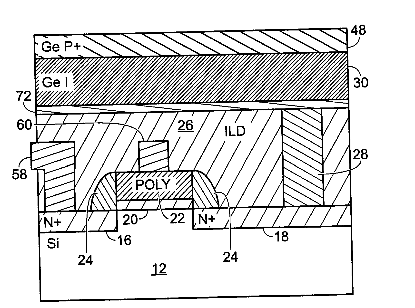
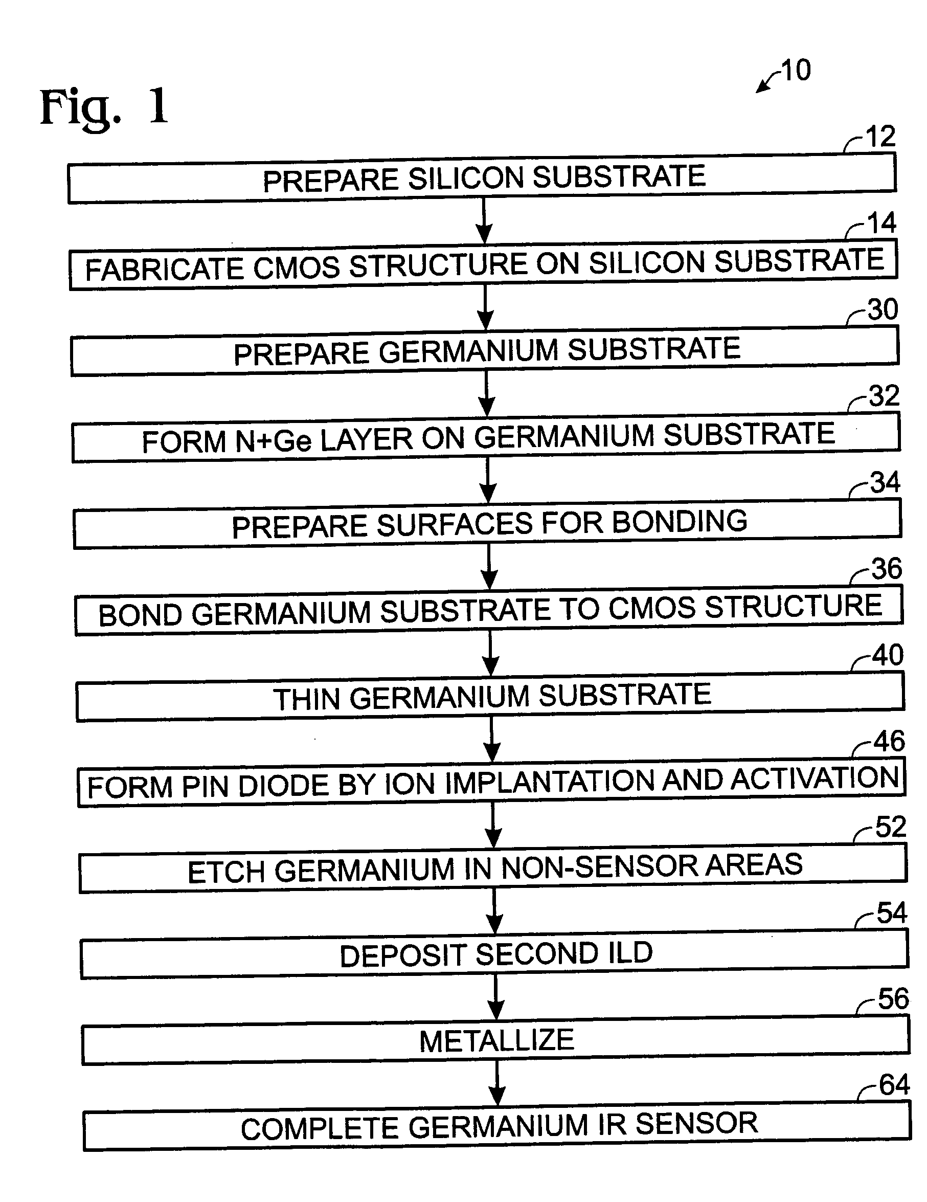
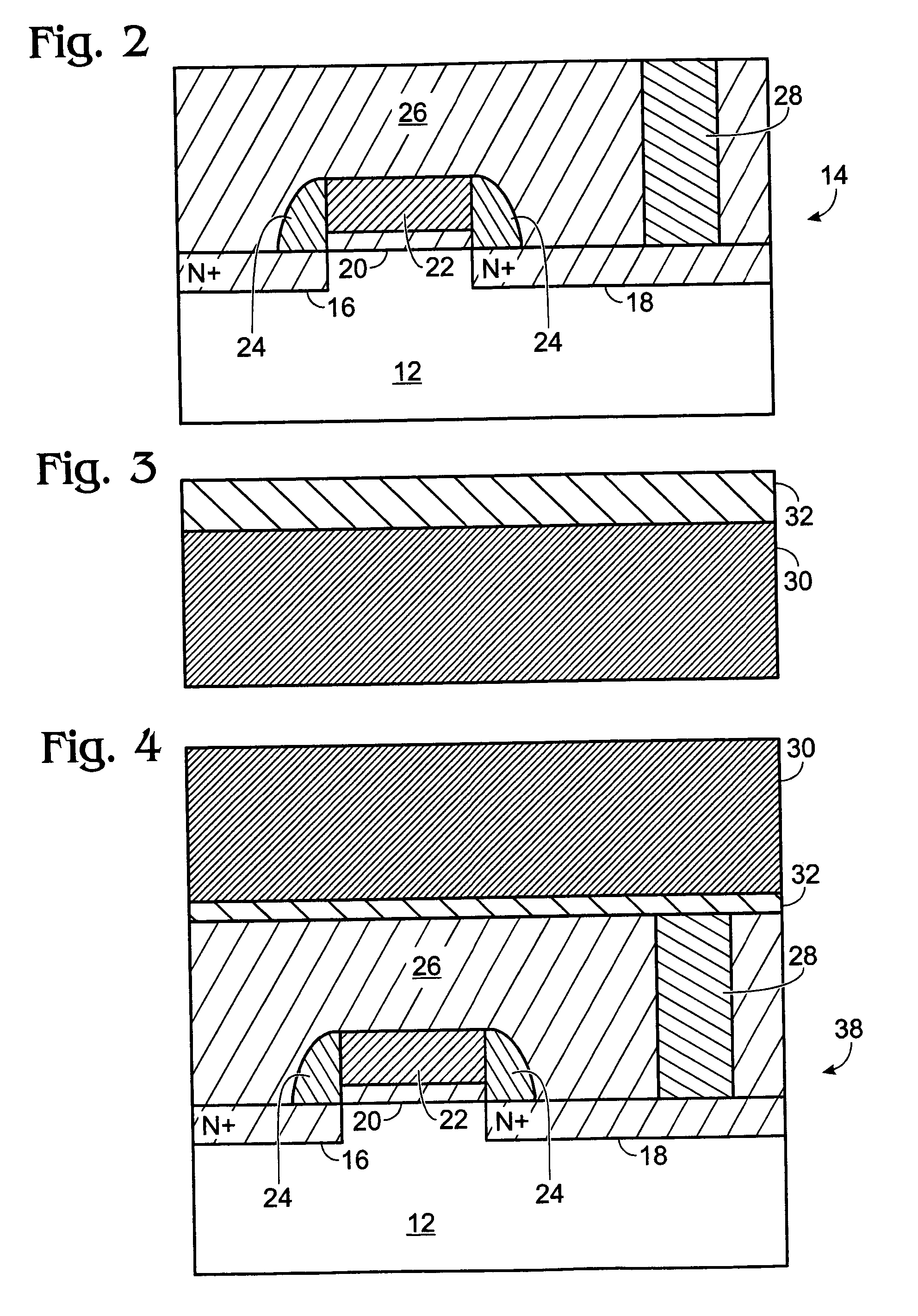
[0018] Using the method of the invention, a germanium thin film is directly bonded to a silicon substrate to preserve the quality of the germanium crystal layer. This invention negates the need for high temperature processes after germanium bonding. High temperature process after bonding results in defects in a germanium thin film, e.g., thermal induced slip, bonding voids and crystalline defect. IC drive circuits are used on a silicon wafer, using standard front-end of line processes before the bonding process takes place. After a germanium thin film is bonded to a silicon wafer, the wafer is only required to undergo standard back-end processes of conventional silicon IC processes, wherein the maximum temperature is between about 300° C. to 400° C. The quality of germanium thin films may thus be preserved and a high efficiency, low noise IR detector may be fabricated. The use of the standard silicon CMOS process in fabrication of the drive circuit also simplifies the fabrication.

[...


PUM

PropertyMeasurementUnit
temperatureaaaaaaaaaa

Abstract

A method of fabricating a thin film germanium photodetector includes preparing a silicon substrate; fabricating a CMOS device on the silicon substrate; preparing a germanium substrate; preparing surfaces of each substrate for bonding; bonding the germanium substrate to the CMOS-bearing silicon substrate to form a bonded structure; removing a portion of the germanium substrate from the bonded structure; forming a PIN diode in the germanium substrate; removing a portion of the germanium layer by etching; and completing the germanium photo detector.

Description

FIELD OF THE INVENTION [0001] This invention relates to photodetectors, and specifically to method of fabricating a germanium based IR sensor. BACKGROUND OF THE INVENTION [0002] Photo detecting in the near-infrared regime, e.g., wavelengths of between about 0.7 μm to 2 μm, has many applications, such as fiber-optical communication, security applications and thermal imaging. Silicon photodiodes are widely used as photodetectors for the visible light regime because of their low dark current and compatibility with silicon integrated circuit technologies. Attempts have been made to deposit Si1-xGex (SiGe) alloys, or germanium thin films, in silicon to fabricate an IR detector, however, the lattice mismatch in a SiGe-to-silicon boundary limits the maximum SiGe thickness which may be formed while still maintaining a defect free structure. Additionally, SiGe thin films having a germanium concentration of less than 50% have a relatively low IR absorption coefficient. Hence, it is difficult ...

Claims


Application Information

Patent Timeline
Patent Type & Authority Applications(United States)
IPC IPC(8): H01L21/00
CPCH01L21/187H01L21/76254H01L27/1443H01L31/0232H01L31/105H01L31/1804Y02E10/547H01L31/02327Y02P70/50
Inventor LEE, JONG-JANMAA, JER-SHENHSU, SHENG TENGTWEET, DOUGLAS J.
Owner SHARP KK
Why Eureka
Try Eureka