Process for producing light-emitting diode element emitting white light

a technology of light-emitting diodes and white light, which is applied in the direction of optical articles, solid-state devices, other domestic articles, etc., can solve the problems of large cost, inevitably formed irregularities at the surface, and considerable increase in manufacturing costs, so as to achieve easy and reliable

Active Publication Date: 2006-06-08
ROHM CO LTD
View PDF5 Cites 37 Cited by
  • Summary
  • Abstract
  • Description
  • Claims
  • Application Information

AI Technical Summary

Benefits of technology

[0019] According to the present invention, an integral LED material plate corresponding to a plurality of LED chips is bonded to the upper surface of an expansion sheet so that either one or both of the cathode electrode and anode electrode of each LED chip of the LED material plate come into close contact with the expansion sheet. After the LED material plate in this state is diced into individual LED chips, the expansion sheet is stretched in two directions which are perpendicular to each other along a surface, whereby the spacing between adjacent LED chips is widened. With such a method, a pitch distance which allows the formation of a predetermined coating on a side surface of each LED chip can be secured between adjacent LED chips.
[0020] Subsequently, after a light-pervious synthetic resin layer containing a fluorescent material is formed on the upper surface of the expansion sheet, the synthetic resin layer is diced to remove portions of the synthetic resin between the LED chips by a cutting width which is smaller than the spacing distance between side surfaces of adjacent LED chips. As a result, the light-pervious synthetic resin containing a fluorescent material remains on the side surfaces of the LED chips. In this way, the side surfaces of each LED chip or the entirety of the chip can be coated with a coating of light-pervious synthetic resin containing a fluorescent material. Further, with such a method, the surface of the coating can be made smooth and flat by dicing, and the thickness of the coating can be made generally uniform with respect to a plurality of LED chips.
[0021] By finally detaching the LED chips from the expansion sheet, either one or both of the cathode electrode and the anode electrode of each LED chip are reliably exposed. Electrical connection of a wiring pattern or a metal wire from the outside to the exposed electrode can be performed easily and reliably.
[0022] In stretching the expansion sheet in two directions which are perpendicular to each other, the stretching dimension in the two directions may be appropriately changed to increase or decrease the spacing between adjacent LED chips and hence to increase or decrease the thickness of the synthetic resin which remains on the side surfaces of LED chips. In this way, the thickness of the coating on each LED chip can be changed as desired.
[0023] Alternatively, in dicing the synthetic resin layer at portions between LED chips, the cutting width in dicing can be appropriately changed to increase or decrease the thickness of the synthetic resin remaining on the side surfaces of LED chips. With such a method again, the thickness of the coating on each LED chip can be changed as desired.
[0024] Alternatively, the changing of the thickness of the coating can be performed by the combination of an appropriate increase or decrease of the stretching dimension in stretching the expansion sheet in two directions and an appropriate increase or decrease of the cutting width in dicing the synthetic resin layer at portions between LED chips.

Problems solved by technology

Therefore, as the pattern mask for photolithography or the mask for screen printing, different kinds of masks need be prepared depending on the number of intended tones, which costs much and results in considerable increase in the manufacturing cost.
Further, by the photolithography of the method (1) and the screen printing of the method (2), irregularities are inevitably formed at the surface of the coating covering the LED chip, and the surface cannot be made a smooth flat surface.
Therefore, the tone of the light becomes non-uniform.
Therefore, changing of the tone is extremely troublesome and requires much cost.

Method used


Image

  • Process for producing light-emitting diode element emitting white light
  • Process for producing light-emitting diode element emitting white light
  • Process for producing light-emitting diode element emitting white light

Examples


first embodiment

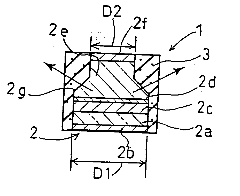
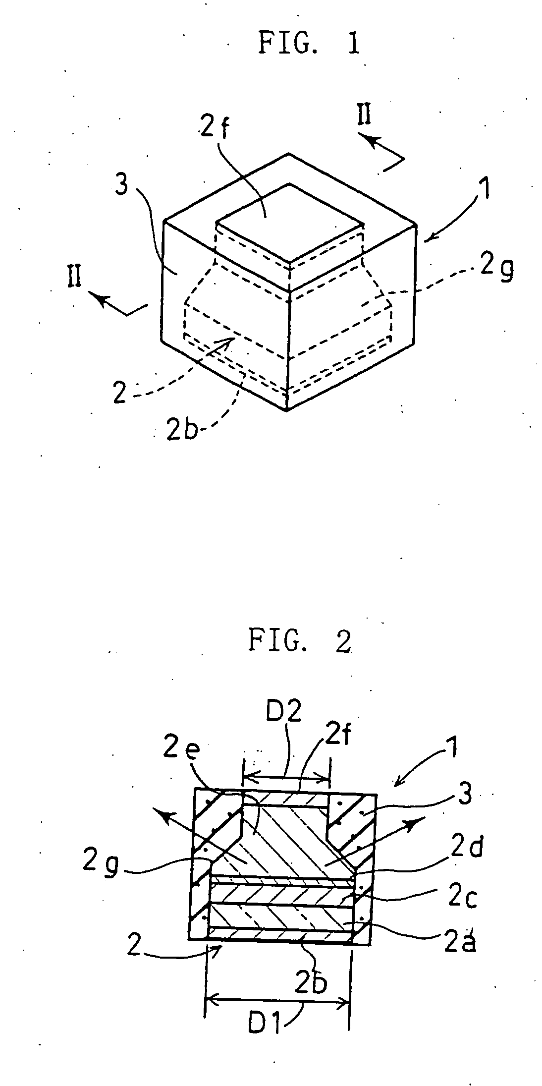
[0061]FIGS. 1-14 show the present invention.

[0062] Of these figures, FIGS. 1 and 2 show an LED element 1 to be manufactured in the first embodiment.

[0063] The LED element 1 includes an LED chip 2, and a coating 3 made of a light-pervious synthetic resin containing a fluorescent material and covering the side surfaces of the LED chip 2. The LED chip 2 includes opposite end surfaces at which an anode electrode 2f and a cathode electrode 2b are provided, respectively, which are exposed without being coated with the coating 3.

[0064] As is conventionally known, the LED chip 2 includes at least a substrate 2a having a lower surface on which the cathode electrode 2b is provided, and an upper surface on which an n-type semiconductor layer 2c, a light-emitting layer 2d for emitting blue light, a p-type semiconductor layer 2e and the anode electrode 2f are stacked.

[0065] In the LED element 1 having the above structure, since the side surfaces of the LED chip 2 are coated with the coating 3...

second embodiment

[0082]FIGS. 15-21 show the present invention.

[0083] Of these figures, FIGS. 15 and 16 show a light-emitting diode element 1′ to be manufactured in the second embodiment.

[0084] The LED element 1′ includes an LED chip 2′ having an end surface at which both of an anode electrode 2f′ and a cathode electrode 2b′ are provided. The entirety of the LED chip 2′ except the end surface provided with the anode electrode 2f′ and the cathode electrode 2b′ is coated with a coating 3′ of a light-pervious synthetic resin containing a fluorescent material.

[0085] As is conventionally known, the LED chip 2′ includes at least a transparent substrate 2a′ made of e.g. sapphire and having a surface on which are stacked an n-type semiconductor layer 2c′, a light-emitting layer 2d′ for emitting blue light, a p-type semiconductor layer 2e′, the cathode electrode 2b′ for the n-type semiconductor layer 2c′, and the anode electrode 2f′ for the p-type semiconductor layer 2e′.

[0086] In the LED element 1′ having...


PUM

PropertyMeasurementUnit
fluorescentaaaaaaaaaa
light emission brightnessaaaaaaaaaa
thicknessaaaaaaaaaa

Abstract

An object of the present invention is to manufacture a white light-emitting diode element by coating a blue light-emitting diode chip with a coating of a synthetic rein containing a fluorescent material. The object is achieved by bonding an LED material plate corresponding to a plurality of LED chips to an expansion sheet, dividing the LED material plate into individual LED chips, stretching the expansion sheet to widen the spacing between the LED chips, forming a synthetic resin layer between the chips, and dicing the synthetic resin layer to remove portions of the synthetic resin layer between the LED chips while leaving part of the synthetic resin layer on a side surface of each of the LED chips.

Description

TECHNICAL FIELD [0001] The present invention relates to a method for manufacturing a light-emitting diode element using a light-emitting diode chip, and particularly to a method for manufacturing a light-emitting diode element that emits white light. BACKGROUND ART [0002] Recently, InGaN-based, blue light-emitting diode chips have been developed, and it is well known that such blue light-emitting diode chips exhibit high light emission brightness. [0003] Such a blue light-emitting diode chip can be utilized for producing white light by coating the surface of the chip with a light-pervious synthetic resin containing a fluorescent material. In this manner, part of the blue light emission is converted into yellow light by the fluorescent material in the coating, and their mixture results in the white light. [0004] In the case where the blue light emitted from a blue light-emitting diode chip is subjected to wavelength conversion for white light emission by coating the chip with a coati...

Claims


Application Information

Patent Timeline
Patent Type & Authority Applications(United States)
IPC IPC(8): B29D11/00C03C15/00H01L21/301H01L33/10H01L33/20H01L33/50H01L33/54H01L33/56H01L33/62
CPCH01L33/20H01L33/505H01L2933/0041H01L2224/48091H01L2224/48247H01L2224/48465H01L2924/00014H01L2924/00
Inventor FUJII, TAKEHIRO
Owner ROHM CO LTD
Why Eureka
Try Eureka