Semiconductor light emitting device and method of manufacturing the same

a technology of semiconductors and light emitting devices, which is applied in the direction of semiconductor devices, basic electric elements, electrical equipment, etc., can solve the problems of high possibility of cracks forming in gan light emitting cells, high cost of silicon substrates, and limited manufacturing size, so as to reduce cracks, reduce light absorption by substrates, and increase the optical output of light emitting devices

Active Publication Date: 2006-06-08
SAMSUNG ELECTRONICS CO LTD
View PDF10 Cites 19 Cited by
  • Summary
  • Abstract
  • Description
  • Claims
  • Application Information

AI Technical Summary

Benefits of technology

[0011] The present invention may provide a semiconductor light emitting device that can minimize cracking in light emitting cells grown on a silicon substrate and effectively increase an optical output of the light emitting device.
[0027] The reflection layer formed on the substrate may reduce the light absorption by the substrate. The height of the light emitting cell may be limited so that light emitted from the light emitting cell can pass through the transparent insulating layer. The transparent insulating layer filling the spaces between the light emitting cells may contribute to the emission of the light to the outside. Accordingly, these methods may reduce cracking in the stacked light emitting cells on the Si substrate, and thus may increase the optical output of the light emitting device.

Problems solved by technology

However, the sapphire substrate is expensive and the manufacturing size is limited.
The light emitting diode having the GaN light emitting cells grown on a silicon substrate has a drawback in that there is a high possibility of cracks forming in the GaN light emitting cells due to the differences in the lattice constant and thermal expansion coefficient between the GaN light emitting cells and the silicon.
However, when the GaN light emitting cells are too thin, their driving voltage becomes too high.
However, the structure requires a complex manufacturing process and, particularly, has a low optical output.

Method used


Image

  • Semiconductor light emitting device and method of manufacturing the same
  • Semiconductor light emitting device and method of manufacturing the same
  • Semiconductor light emitting device and method of manufacturing the same

Examples


Embodiment Construction

[0038] A semiconductor light emitting diode and a method of manufacturing the semiconductor light emitting diode according to the present invention will now be described more fully with reference to the accompanying drawings, in which exemplary embodiments of the invention are shown. In the drawings, the thicknesses of layers and regions are exaggerated for clarity.

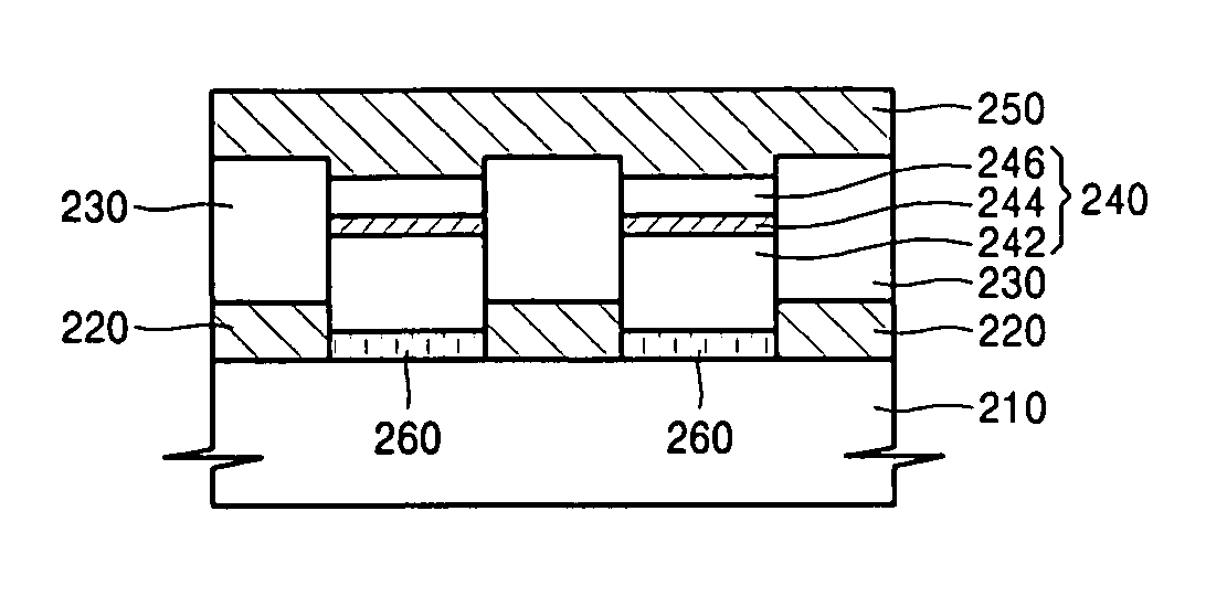
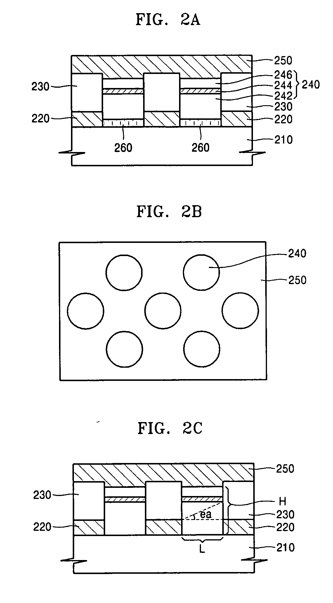
[0039]FIG. 2A is a cross-sectional view of a semiconductor light emitting device according to an embodiment of the present invention.

[0040] Referring to FIG. 2A, a semiconductor light emitting device includes a substrate 210, at least two light emitting cells 240 located on the substrate 210 and formed by stacking semiconductor material layers, a reflection layer 220 and a transparent insulating layer 230 sequentially stacked between the light emitting cells 240, and a transparent electrode 250 covering the upper surfaces of the light emitting cells 240. The substrate 210 can be formed of silicon Si.

[0041] The reflecti...


PUM


Abstract

A semiconductor light emitting device and a method of manufacturing the semiconductor light emitting device are provided. The semiconductor light emitting device includes a substrate, at least two light emitting cells located on the substrate and formed by stacking semiconductor material layers, a reflection layer and a transparent insulating layer sequentially stacked between the light emitting cells, and a transparent electrode covering the upper surface of the light emitting cells.

Description

CROSS-REFERENCE TO RELATED PATENT APPLICATION [0001] This application claims the benefit of Korean Patent Application No. 10-2004-0100354, filed on Dec. 2, 2004, in the Korean Intellectual Property Office, the disclosure of which is incorporated herein in its entirety by reference. BACKGROUND OF THE DISCLOSURE [0002] 1. Field of the Disclosure [0003] The present disclosure relates to a semiconductor light emitting device and a method of manufacturing the same, and more particularly, to a semiconductor light emitting device composed of a plurality of light emitting cells and a reflection film, and a method of manufacturing the same. [0004] 2. Description of the Related Art [0005] Light emitting diodes (LEDs) are widely used as a means for transmitting, recording, or reading data in communication devices, such as optical communication devices, or in electronic devices, such as compact disc players (CDPs) and digital versatile disc players (DVDPs). The LEDs are expanding in application...

Claims


Application Information

Patent Timeline
Patent Type & Authority Applications(United States)
IPC IPC(8): H01L33/00H01L33/08H01L33/10H01L33/12H01L33/32H01L33/34H01L33/38H01L33/42
CPCH01L25/0753H01L27/153H01L33/0079H01L33/32H01L33/42H01L33/46H01L2924/0002H01L33/0093H01L2924/00
Inventor LEE, JEONG-WOOK
Owner SAMSUNG ELECTRONICS CO LTD
Why Eureka
Try Eureka