
Damascene interconnect structure with cap layer

Active Publication Date: 2006-06-08
TAIWAN SEMICON MFG CO LTD
View PDF6 Cites 63 Cited by
  • Summary
  • Abstract
  • Description
  • Claims
  • Application Information

AI Technical Summary

Benefits of technology

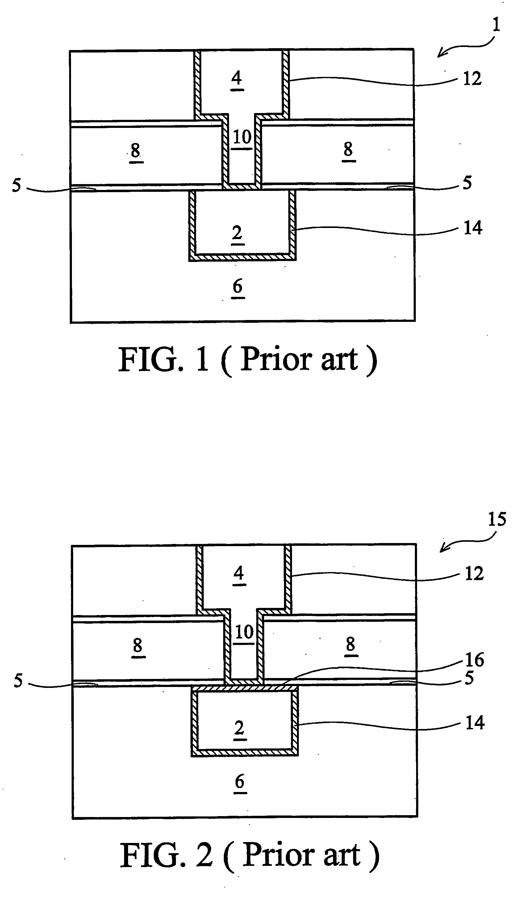
[0011] With a conductive cap on the first conductive line, the reliability and performance of the interconnection structure is significantly improved. The preferred embodiment of the present invention eliminates the possibility that the second conductive line is coupled to the first conductive line through the cap layer, which causes higher contact resistance and thus higher RC delay.

Problems solved by technology

However, copper still suffers from electro migration (EM) and stress migration (SM) reliability issues as geometries continue to shrink, and current densities increase.
The interconnection structure 1 in FIG. 1 suffers from electro migration and stress migration problems.
However, the introduction of the cap layer 16 generates another problem.
Therefore, contact resistance and RC delay varies from process to process and is harder to predict.

Method used


Image

  • Damascene interconnect structure with cap layer
  • Damascene interconnect structure with cap layer
  • Damascene interconnect structure with cap layer

Examples


Embodiment Construction

[0016] The making and using of the presently preferred embodiments are discussed in detail below. It should be appreciated, however, that the present invention provides many applicable inventive concepts that can be embodied in a wide variety of specific contexts. The specific embodiments discussed are merely illustrative of specific ways to make and use the invention, and do not limit the scope of the invention.

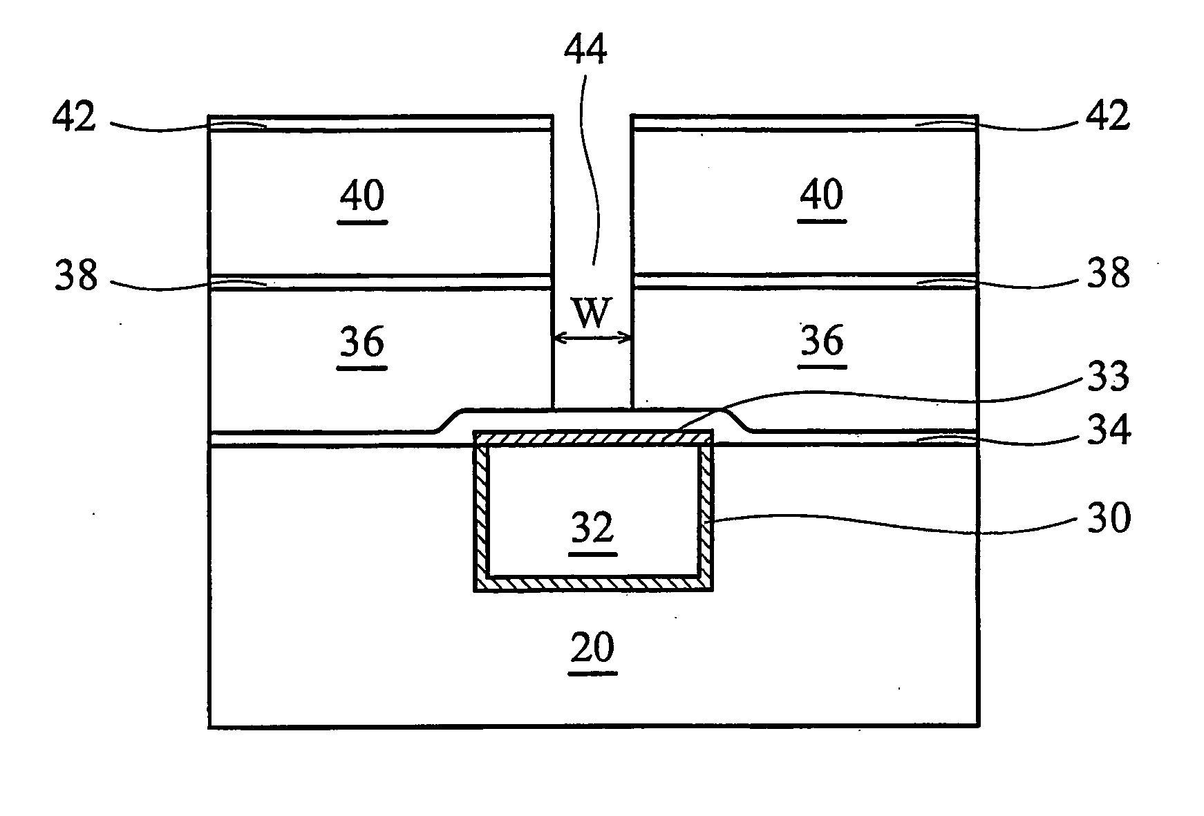
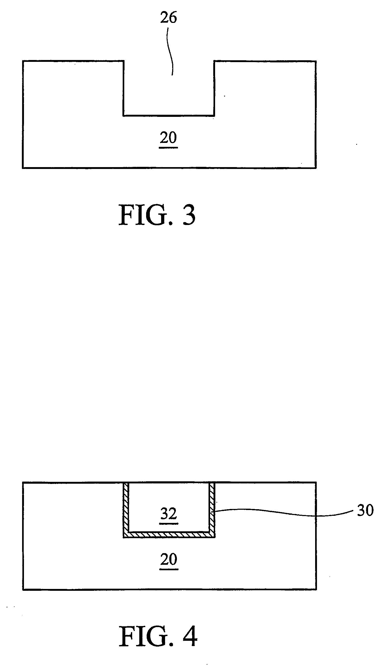
[0017]FIGS. 3 through 10 are cross-sectional views of intermediate stages in the making of a preferred embodiment of the present invention. A via connecting two conductive lines are formed. FIG. 3 illustrates formation of a trench 26 in a base material 20. In the preferred embodiment, base material 20 is an IMD preferably comprising a material having a dielectric constant (K value) lower than about 3.3 and contains nitrogen, carbon, hydrogen, oxygen, fluorine and their combinations. In alternative embodiments, base material 20 can be a silicon substrate or other non-conduct...


PUM


Abstract

A method of forming an integrated circuit interconnect structure is presented. A first conductive line is formed over a semiconductor substrate. A conductive cap layer is formed on the first conductive line to improve device reliability. An etch stop layer (ESL) is formed on the conductive cap layer. An inter-level dielectric (IMD) is formed on the ESL. A via opening and a trench are formed in the ESL, IMD, and conductive cap layer. A recess is formed in the first conductive line. The recess can be formed by over etching when the first dielectric is etched, or by a separate process such as argon sputtering. A second conductive line is formed filling the trench, opening and recess.

Description

TECHNICAL FIELD [0001] This invention relates generally to metallization of the integrated circuit, and more specifically to damascene process. BACKGROUND [0002] Conventional integrated circuit contains a plurality of patterns of metal lines separated by inter-wiring spacings, and a plurality of interconnect lines, such as bus lines, bit lines, word lines and logic interconnect lines. Typically, the metal patterns of vertically spaced metallization layers are electrically interconnected by vias. Metal lines formed in trench-like openings typically extend substantially parallel to the semiconductor substrate. Semiconductor devices of such type according to current technology may comprise eight or more levels of metallization to satisfy device geometry and micro miniaturization requirements. [0003] A common method for forming metal lines or plugs is known as “damascene”. Generally, this process involves forming an opening in the dielectric interlayer, which separates the vertically sp...

Claims


Application Information

Patent Timeline
IPC IPC(8): H01L23/48H01L23/52
CPCH01L21/76805H01L21/76807H01L21/76834H01L21/76838H01L23/5226H01L2924/0002H01L23/53238H01L23/53295H01L2924/00
Inventor HUANG, JUI JENTSAI, MINGHSINGSHUE, SHAU-LINSU, HUNG-WENKO, TING-CHU
Owner TAIWAN SEMICON MFG CO LTD
Learn More