
Self-timed switching regulator pre-driver

Active Publication Date: 2006-06-08
ANALOG DEVICES INC
View PDF14 Cites 10 Cited by
  • Summary
  • Abstract
  • Description
  • Claims
  • Application Information

AI Technical Summary

Benefits of technology

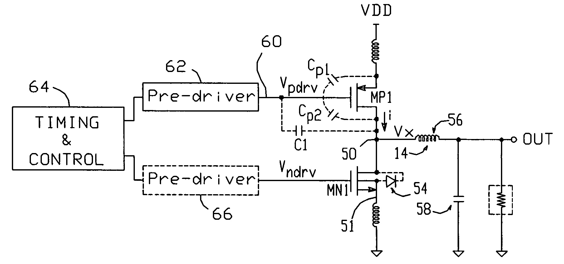
[0010] A switching regulator pre-driver circuit is presented which overcomes the problems noted above, providing a regulator with lower di / dt-induced switching noise and higher efficiency when compared with prior art regulators.
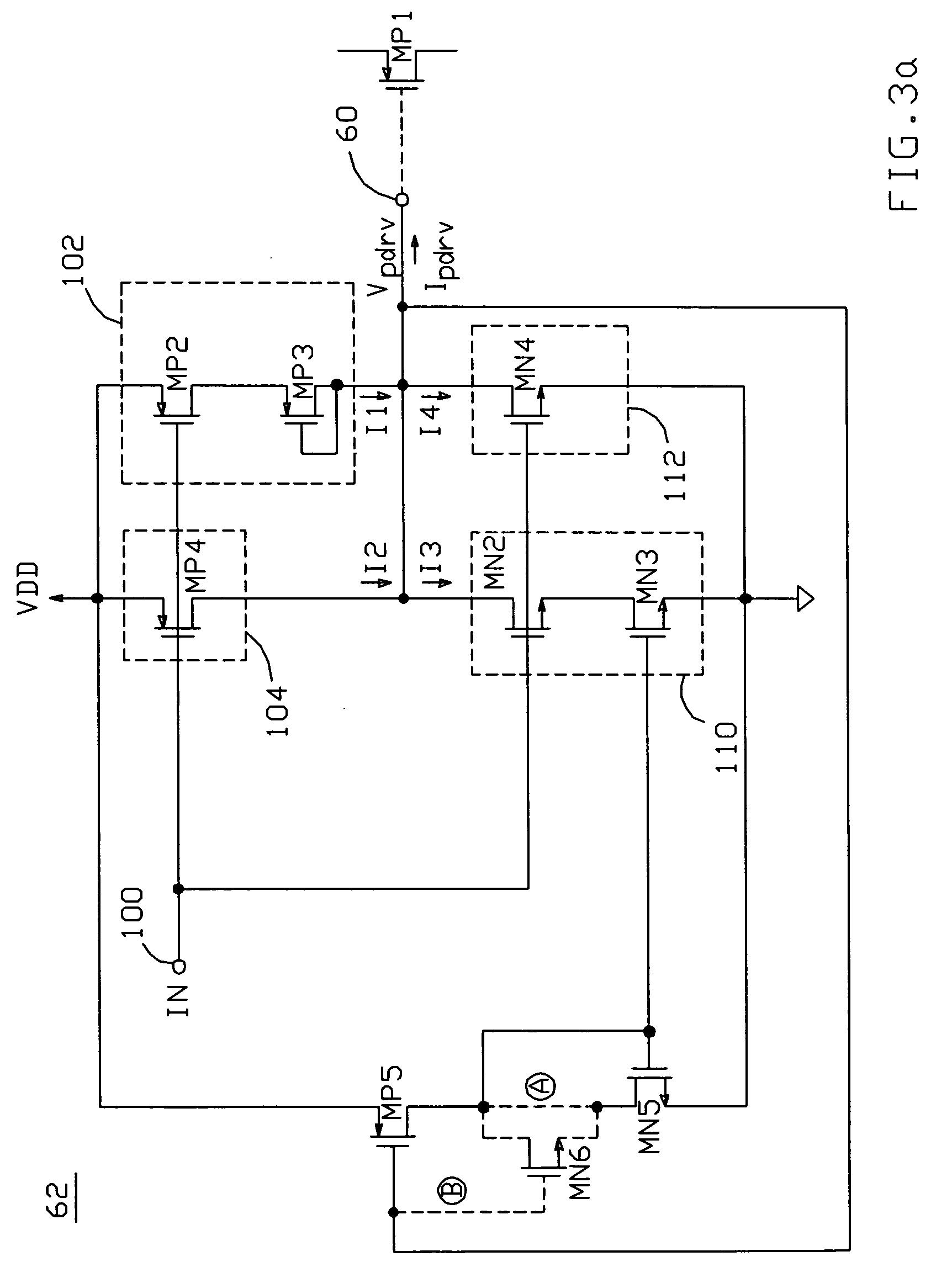
[0012] The control signal provided by the pre-driver circuit has an associated voltage Vdrv, which the pre-driver pulls up and down with a current Idrv to cycle the switching transistor on and off. The pre-driver circuit is arranged to adaptively vary Idrv such that current Idrv is at a relatively low level when the rate of change of current i (di / dt) in the switching transistor is relatively high, and such that current Idrv is at a relatively high level when di / dt is relatively low. Adaptively adjusting Idrv in this way limits di / dt-induced noise at the circuit common point.
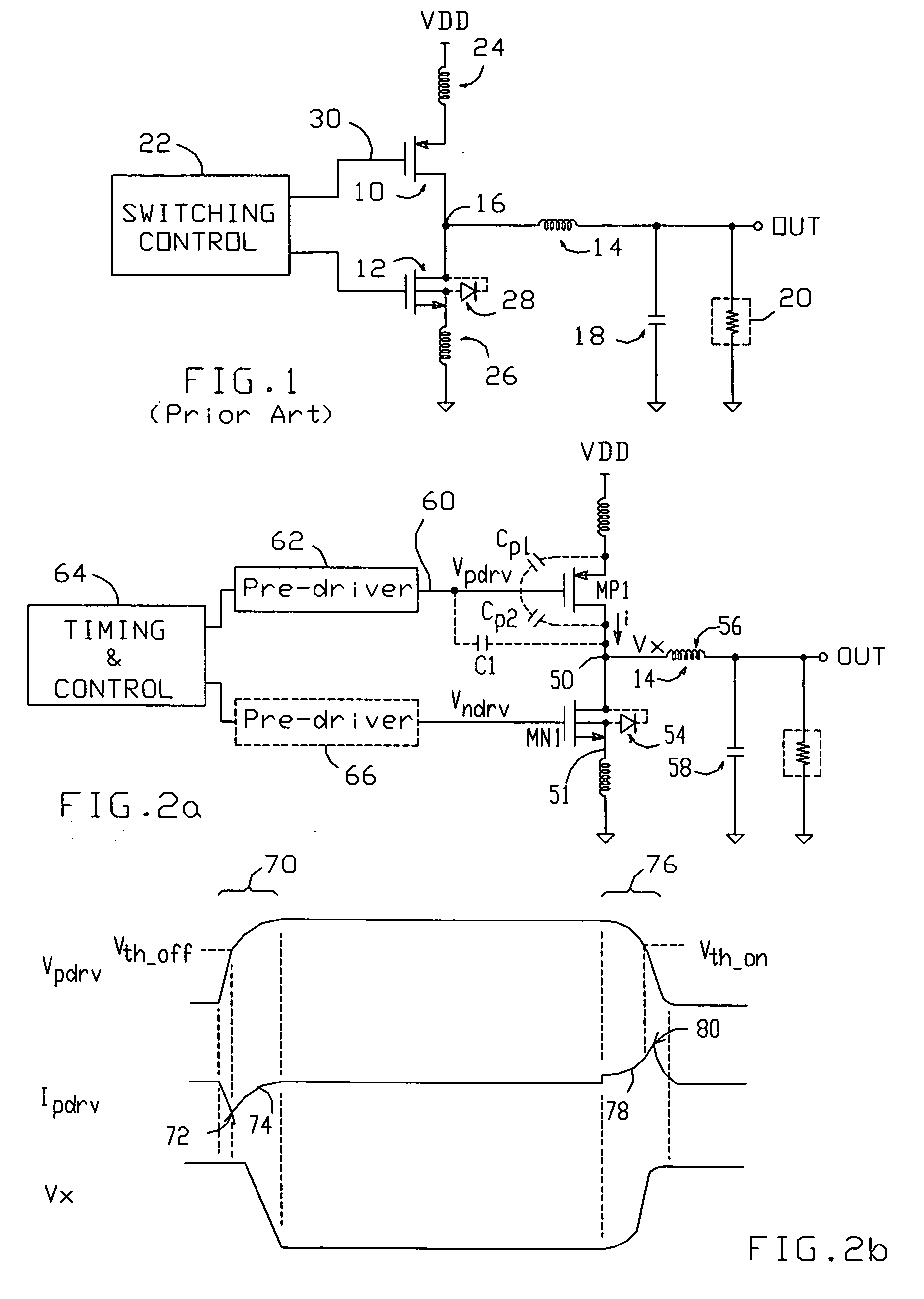
[0013] The pre-driver circuit is implemented such that, when a p-type switching transistor is being cycled on, current Idrv is at a relatively low level when Vdrv is greater than a first threshold voltage, and at a relatively high level when Vdrv is less than the first threshold voltage. When cycling the transistor off, current Idrv is at a relatively high level when Vdrv is less than a second threshold voltage, and at a relatively low level when Vdrv is greater than the second threshold voltage. Di / dt-induced noise is reduced by deriving the threshold voltages from transistors within the pre-driver circuit which emulate the behavior of the switching transistor, so that control signal slew rate is reduced when di / dt would otherwise be at its greatest.

Problems solved by technology

An inherent problem common to all switching voltage regulators is switching noise generated by cycling the regulator's switching transistor(s) on and off.
This is particularly troublesome when integrating precision analog blocks on the same substrate as the regulator: it is difficult to isolate the analog blocks from the switching noise, which can disturb analog signals inductively, capacitively or resistively.
However, this may consume an unacceptable amount of area on the chip.
Unfortunately, this will require a very high switching frequency when used near wideband analog signals; as a result, the di / dt and dv / dt of the switched signals also increases, as does the magnitude of the switching noise.
However, since the energy of the switching noise is more or less distributed in each switching period, and since there are potentially multiple coupling paths, the benefit of synchronization may be limited.
This results in a large voltage drop being developed across the bond wires (V=L*di / dt).
However, a slow slew rate has an adverse effect on the efficiency of the regulator: a slow transition results in transistors 10 and 12 operating in a higher on-resistance region for a longer time, thus lowering efficiency.

Method used


Image

  • Self-timed switching regulator pre-driver
  • Self-timed switching regulator pre-driver
  • Self-timed switching regulator pre-driver

Examples


Embodiment Construction

[0023] A diagram depicting a switching regulator in accordance with the present invention is shown in FIG. 2a. The regulator includes a switching transistor MP1, here a PMOS FET (though the invention is equally useful with both n and p-type FETs and BJTs), connected between a supply voltage VDD and a node 50; MP1 conducts a current i to node 50. The regulator also includes circuitry 52 which provides a conductive path between node 50 and a circuit common point 51 (typically connected to ground via a bond wire); in the exemplary embodiment shown in FIG. 2a, circuitry 52 comprises a second switching transistor MN1 (with its intrinsic body diode 54). For the exemplary synchronous buck-type regulator shown in FIG. 2a, an output inductor 56 would typically be connected between node 50 and the regulator's output terminal OUT, and a filter capacitor 58 would typically be connected between OUT and ground.

[0024] Switching transistor MP1 is cycled on and off in response to a control signal 6...


PUM


Abstract

A switching voltage regulator includes a switching transistor connected to conduct a current (i) between a supply voltage and a first node in response to a control signal which cycles the transistor on and off, and a “pre-driver” circuit which provides the control signal. The control signal is pulled up and down with a current Idrv. The pre-driver circuit adaptively varies Idrv such that it is at a relatively low level when the rate of change of current i (di / dt) in the switching transistor is relatively high, and is at a relatively high level when di / dt is relatively low.

Description

BACKGROUND OF THE INVENTION [0001] 1. Field of the Invention [0002] This invention relates to the field of switching voltage regulators, and particularly to circuits for reducing di / dt noise in such regulators. [0003] 2. Description of the Related Art [0004] An inherent problem common to all switching voltage regulators is switching noise generated by cycling the regulator's switching transistor(s) on and off. This is particularly troublesome when integrating precision analog blocks on the same substrate as the regulator: it is difficult to isolate the analog blocks from the switching noise, which can disturb analog signals inductively, capacitively or resistively. [0005] Several well-known techniques are available to reduce or prevent switching noise from affecting analog performance. For example, the physical spacing between the switching regulator and the analog blocks can be increased. However, this may consume an unacceptable amount of area on the chip. Alternatively, the regul...

Claims


Application Information

Patent Timeline
IPC IPC(8): G05F1/656
CPCH02M1/08H02M1/44H03K17/164G05F1/656
Inventor JIANG, XUESONG
Owner ANALOG DEVICES INC
Learn More