
Semiconductor device and method for fabricating the same

a semiconductor and semiconductor technology, applied in the field of semiconductor devices, can solve the problems of difficulty in electrically connecting or integrating a plurality of elements (hfets) formed on one semiconductor substrate, and achieve the effects of reducing interconnect resistance, higher voltage, and reducing interconnect resistan

Active Publication Date: 2006-06-15
PANASONIC CORP
View PDF18 Cites 42 Cited by
  • Summary
  • Abstract
  • Description
  • Claims
  • Application Information

AI Technical Summary

Benefits of technology

[0015] In the first semiconductor device, each of the semiconductor elements preferably has at least one terminal, and at least one of the semiconductor elements is preferably electrically connected to the semiconductor substrate at the terminal. Thus, the semiconductor substrate connected to one terminal of the semiconductor element functions as a field plate for releasing the electric field, and therefore, a higher breakdown voltage can be attained. Furthermore, since the semiconductor substrate has the same potential with respect to the plural semiconductor elements, if the semiconductor substrate is connected to a terminal for supplying common potential to the semiconductor elements, such as ground potential, a ground interconnect can be reduced.
[0028] The second semiconductor device preferably further includes an insulating isolation region formed in the semiconductor substrate around the semiconductor elements. Thus, the breakdown voltage between the semiconductor elements can be increased, and hence, the semiconductor device can be operated at a higher voltage.

Problems solved by technology

Conventionally, such devices are developed as simplex devices for attaining performances that are realized by utilizing good material characteristics (physical properties) of a group III-V nitride semiconductor itself but cannot be realized by using other materials.
In the conventional group III-V nitride semiconductor device, however, current leakage is caused through the semiconductor substrate 101 in a high voltage operation, and therefore, it is difficult to electrically connecting or integrating a plurality of elements (HFETs) formed on one semiconductor substrate 101.

Method used


Image

  • Semiconductor device and method for fabricating the same
  • Semiconductor device and method for fabricating the same
  • Semiconductor device and method for fabricating the same

Examples


embodiment 1

[0042] Embodiment 1 of the invention will now be described with reference to the accompanying drawings.

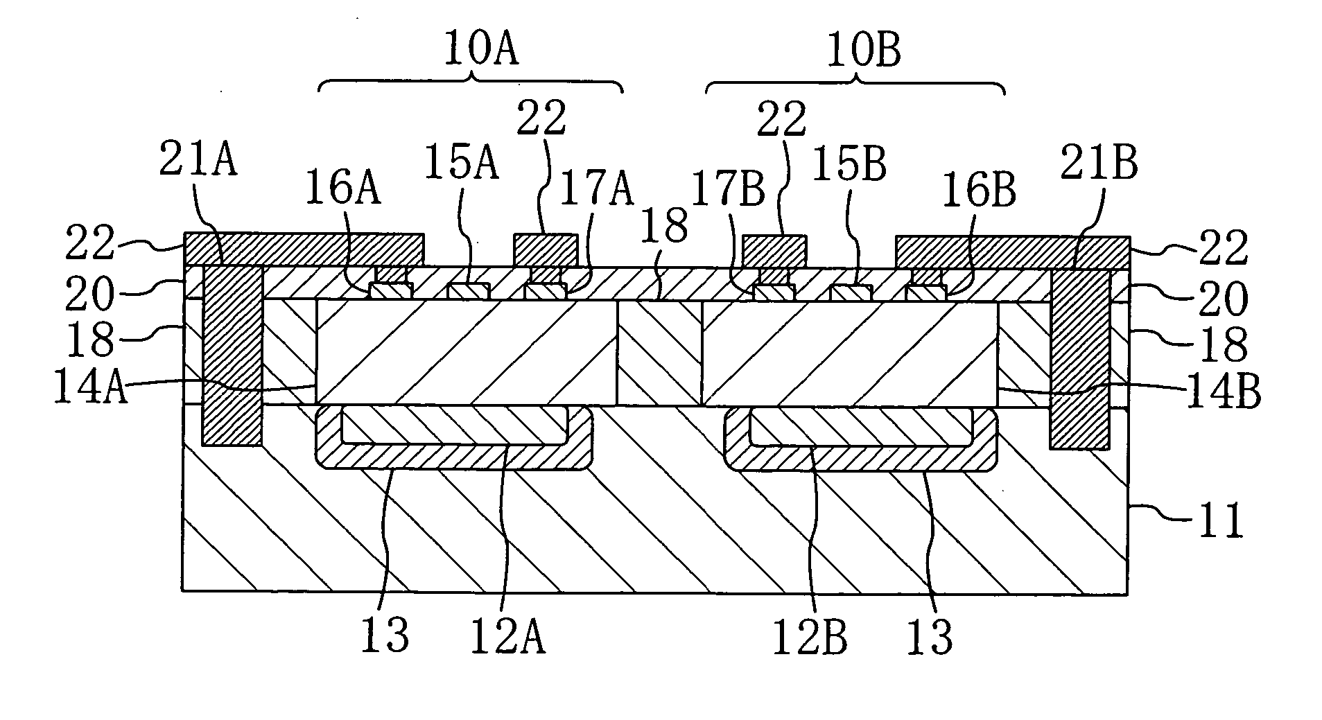
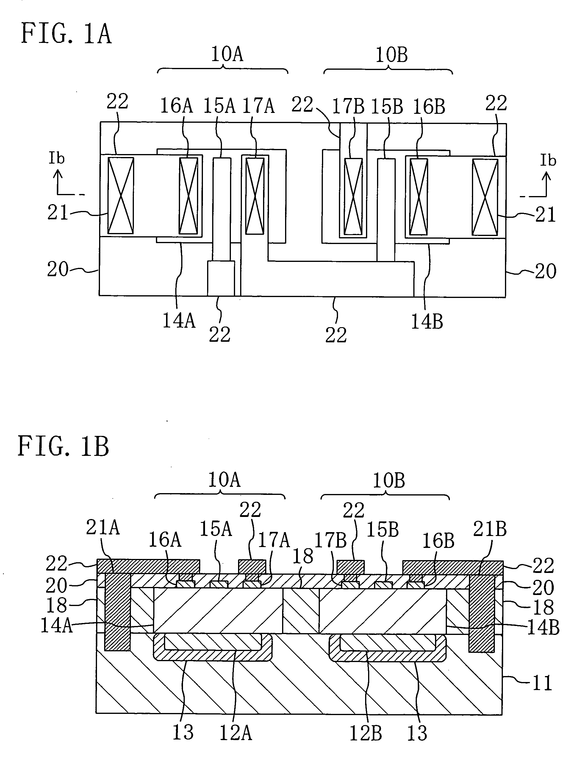
[0043]FIGS. 1A and 1B show a semiconductor device of Embodiment 1 in which two high power HFETs are integrated, and specifically, FIG. 1A is a plan view thereof and FIG. 1B is a cross-sectional view thereof taken on line Ib-Ib of FIG. 1A.

[0044] As shown in FIG. 1B, a first polarity inversion region 12A and a second polarity inversion region 12B both of p-type conductivity spaced from each other are selectively formed in an upper portion of a semiconductor substrate 11 of, for example, n-type silicon (Si). The bottoms and the side faces of the polarity inversion regions 12A and 12B are covered with a p-type low concentration impurity region 13 including a p-type impurity in a lower concentration than in the polarity inversion regions 12A and 12B. Since the p-type low concentration impurity region 13 is thus provided, a larger depletion layer extends in the semiconductor substrate ...

embodiment 2

[0063] Embodiment 2 of the invention will now be described with reference to the accompanying drawings.

[0064]FIG. 7 is a cross-sectional view of a semiconductor device of Embodiment 2 in which two high power HFETs are integrated. The plan structure of this semiconductor device is similar to that of Embodiment 1 shown in FIG. 1B. Also, like reference numerals are used in FIG. 7 to refer like elements shown in FIG. 1 and the description is omitted.

[0065] In Embodiment 1, the semiconductor substrate 11 of n-type silicon is used as the substrate on which the group III-V nitride semiconductor layer 14 is epitaxially grown.

[0066] In contrast, an n-type SOI substrate 31 including an n-type upper silicon layer 30a, a buried oxide layer 30b and an n-type lower silicon layer 30c is used in Embodiment 2 as shown in FIG. 7.

[0067] Specifically, the SOI substrate 31 includes the n-type upper silicon layer 30a with a thickness of 0.2 μm, the buried oxide layer 30b of silicon oxide with a thick...


PUM


Abstract

A semiconductor device includes a semiconductor substrate of n-type silicon including, in an upper portion thereof, a first polarity inversion region and a second polarity inversion regions spaced from each other and doped with a p-type impurity. A first HFET including a first active layer and a second HFET including a second active layer both made of a group Ill-V nitride semiconductor are independently formed on the respective polarity inversion regions in the semiconductor substrate, and the HFETs are electrically connected to each other through interconnects.

Description

CROSS-REFERENCE TO RELATED APPLICATIONS [0001] This application claims priority under 35 U.S.C. § 119 on Patent Application Nos. 2004-359447 and 2005-316247 filed in Japan respectively on Dec. 13, 2004 and Oct. 31, 2005, the entire contents of which are hereby incorporated by reference. BACKGROUND OF THE INVENTION [0002] The present invention relates to a semiconductor device and a method for fabricating the same, and more particularly it relates to a semiconductor device including a plurality of high power elements using a group III-V nitride semiconductor. [0003] A group III-V nitride semiconductor is a compound semiconductor of a compound composed of aluminum (Al), boron (B), gallium (Ga) or indium (In) and nitride (N) represented by a general formula of BwAlxGayInzN (wherein w+x+y+z=1 and 0≦w, x, y, z≦1). [0004] A group III-V nitride semiconductor has various advantages such as a large band gap, a high breakdown voltage derived from the large band gap, a high electron saturation...

Claims


Application Information

Patent Timeline
IPC IPC(8): H01L31/109
CPCH01L21/84H01L27/0605H01L27/1203H01L29/2003H01L29/66462H01L29/7787
Inventor HIROSE, YUTAKATANAKA, TSUYOSHI
Owner PANASONIC CORP
Learn More