Modularized probe card for high frequency probing

a probe card and high frequency technology, applied in the field of probe cards, can solve the problems of ineffective decoupling apparatus, complex circuit design of probe cards, and loss, and achieve the effect of reducing the cost of the probe head made of ceramic substrates, and reducing the cost of the probe head

Inactive Publication Date: 2006-06-15
CHIPMOS TECH INC
View PDF12 Cites 32 Cited by
  • Summary
  • Abstract
  • Description
  • Claims
  • Application Information

AI Technical Summary

Benefits of technology

[0004] A main purpose of the present invention is to provide a modularized probe card for high frequency probing. It mainly includes a probe head, a mounting board and an interposer. There are a plurality of cavities on the back surface of the probe head for deposing a plurality of decoupling components which are connecting to the power plane and the ground plane of the probe head. The power plane and the ground plane of the probe head are respectively connected to the power plane and the ground plane of the mounting board through a plurality of power and ground circuitry inside the probe head, then through a plurality of contact pads on the back surface of the probe head which are connected to the contact ends on the bottom surface of the interposer, then t

Problems solved by technology

For multiple DUT probing, the circuit design of a probe card becomes more complicated than ever.
Without accurate EMI control in a probe card, the testing results may

Method used


Image

  • Modularized probe card for high frequency probing
  • Modularized probe card for high frequency probing
  • Modularized probe card for high frequency probing

Examples


Embodiment Construction

[0007] Please refer to the drawings attached, present invention will be described by means of an embodiment below.

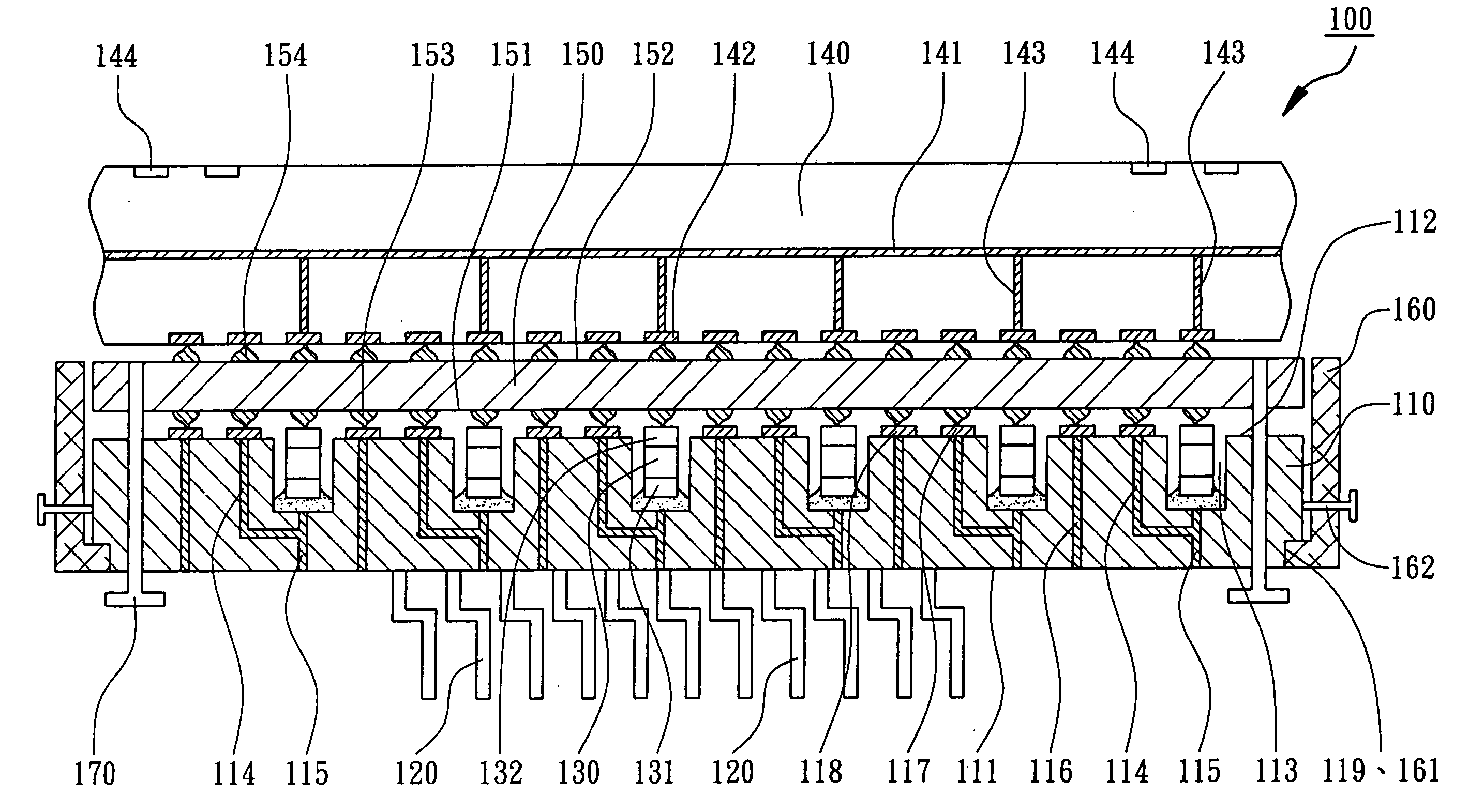
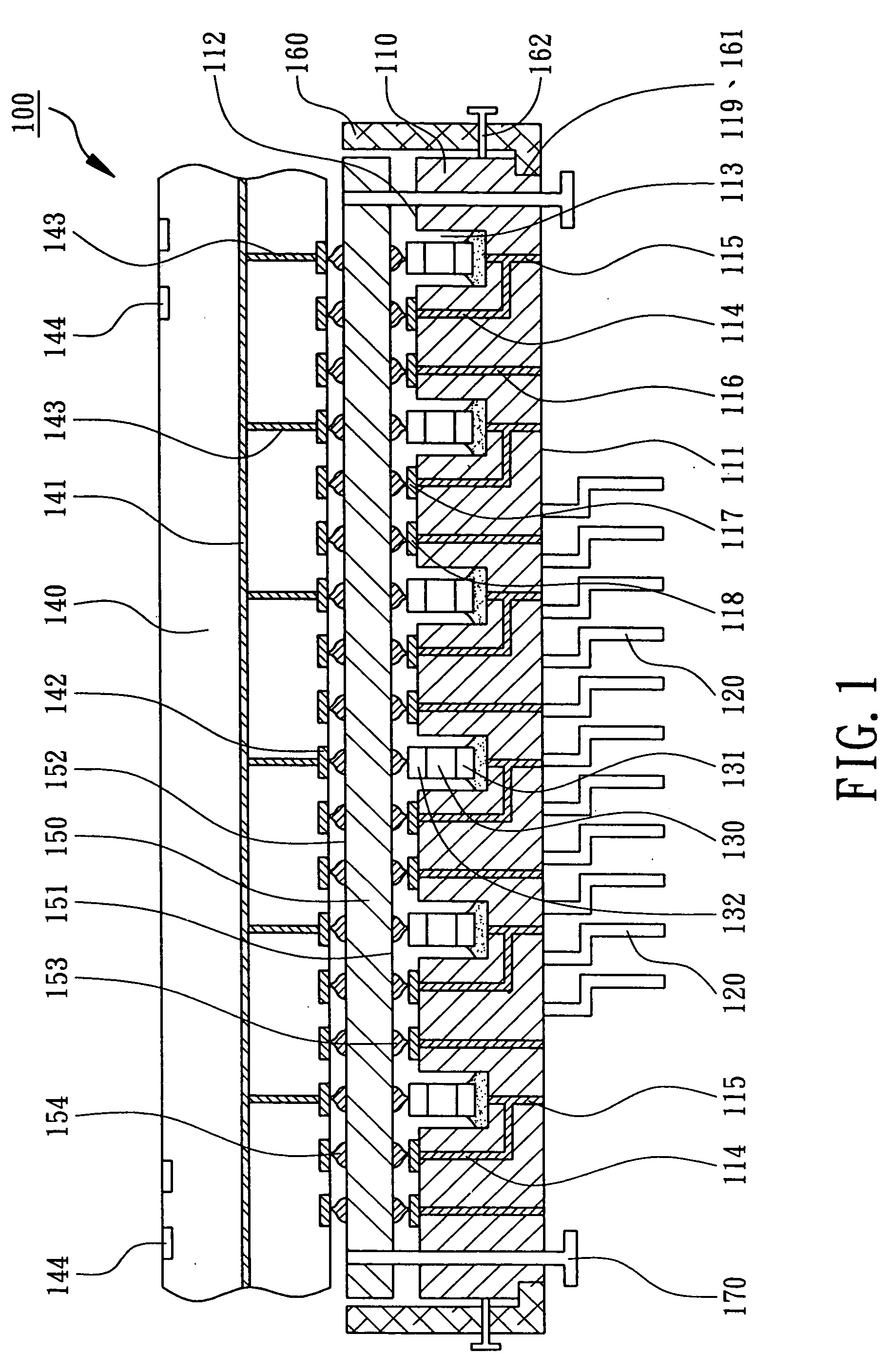
[0008] According to the present invention, a modularized probe card 100 mainly comprises a probe head 110 with probes 120, a plurality of decoupling components 130, a mounting board 140 and an interposer 150. In this embodiment, the probe head 110 is a multi-layer ceramic substrate; however, it can be a glass substrate, a Si wafer, or a PCB according to the CTE of the devices under test. The probe head 110 has a probing surface 111 and a corresponding back surface 112. A plurality of cavities 113 are formed on the back surface 112, preferably, the cavities 113 are arranged in an array. The probe head 110 includes a plurality of power / ground circuitries 114, a plurality of bypass circuitries 115, and a plurality of signal circuitries 116. A plurality of power / ground pads 117 and a plurality of signal pads 118 are formed on the back surface 112 of the probe head 110. The ...


PUM


Abstract

A modularized probe head for high frequency probing is provided. The probe head mainly includes a probe head, a mounting board and an interposer between the probe head and the mounting board. The probe head has a plurality of cavities on its back surface. A plurality of decoupling components are installed inside the cavities and are electrically coupled to the ground/power circuitry of the probe head via by-pass circuitry. The interposer has a bottom surface corresponding to the back surface of the probe head, and includes a plurality of contact ends on the bottom surface. Some of the contact ends electrically contact the decoupling components and electrically coupled to the ground plane of the mounting board.

Description

FIELD OF THE INVENTION [0001] The present invention relates to a probe card configured for probing a semiconductor wafer under test, and more particularly to a probe card for high frequency probing. BACKGROUND OF THE INVENTION [0002] The development of semiconductor devices is always walking toward higher density and higher frequency. Conventionally, a probe card is mounted on the test head of a tester for chip probing semiconductor devices in wafer form. In order to save the testing cost and to increase the testing throughput, multiple DUT (device under test) probing is required and developed. For multiple DUT probing, the circuit design of a probe card becomes more complicated than ever. Moreover, the EMI (Electro-Magnetic Interference) will become a dominant factor in high frequency probing. Without accurate EMI control in a probe card, the testing results may be misleading and causing yields loss. [0003] A probe card assembly had been disclosed in the U.S. Pat. No. 5,491,426. A ...

Claims


Application Information

Patent Timeline
IPC IPC(8): G01R31/02
CPCG01R31/2822G01R31/2889G01R1/07378
Inventor LIU, AN-HONGWANG, YEONG-HERCHAO, YEONG-CHINGLEE, YAO-JUNG
Owner CHIPMOS TECH INC
Why Eureka
Try Eureka