Inductor, resonant circuit, semiconductor integrated circuit, oscillator, and communication apparatus

a resonant circuit and semiconductor technology, applied in the direction of transformer/inductance details, oscillators, inductance generators, etc., can solve the problems of increasing the area of the circuit, increasing the area of the inductor, etc., to reduce the efficiency of the reduction of wiring resistance and reduce the parasitic capacitance. the effect of increasing the parasitic capacitance due to the multi-layered coil pattern

Inactive Publication Date: 2006-06-15
SHARP KK
View PDF6 Cites 30 Cited by
  • Summary
  • Abstract
  • Description
  • Claims
  • Application Information

AI Technical Summary

Benefits of technology

[0019] In this manner, when the inductor of the present invention is employed in the resonant circuit, in which the variable capacitance device and the inductor are supposed to be provided in parallel, the effect of the increased parasitic capacitance due to the multilayered coil patterns is reduced. Further, reduction efficiency of the wiring resistance is significantly increased by the multilayered coil patterns. As a result, a resonant circuit is realized which has a high Q.

Problems solved by technology

As such, a reduction in Q of the resonant circuit causes an increase in the phase noise.
However, this results in increasing the area of the inductor, and further increasing the area of the circuit.

Method used


Image

  • Inductor, resonant circuit, semiconductor integrated circuit, oscillator, and communication apparatus
  • Inductor, resonant circuit, semiconductor integrated circuit, oscillator, and communication apparatus
  • Inductor, resonant circuit, semiconductor integrated circuit, oscillator, and communication apparatus

Examples


Embodiment Construction

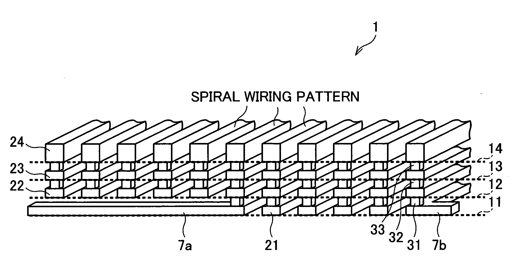
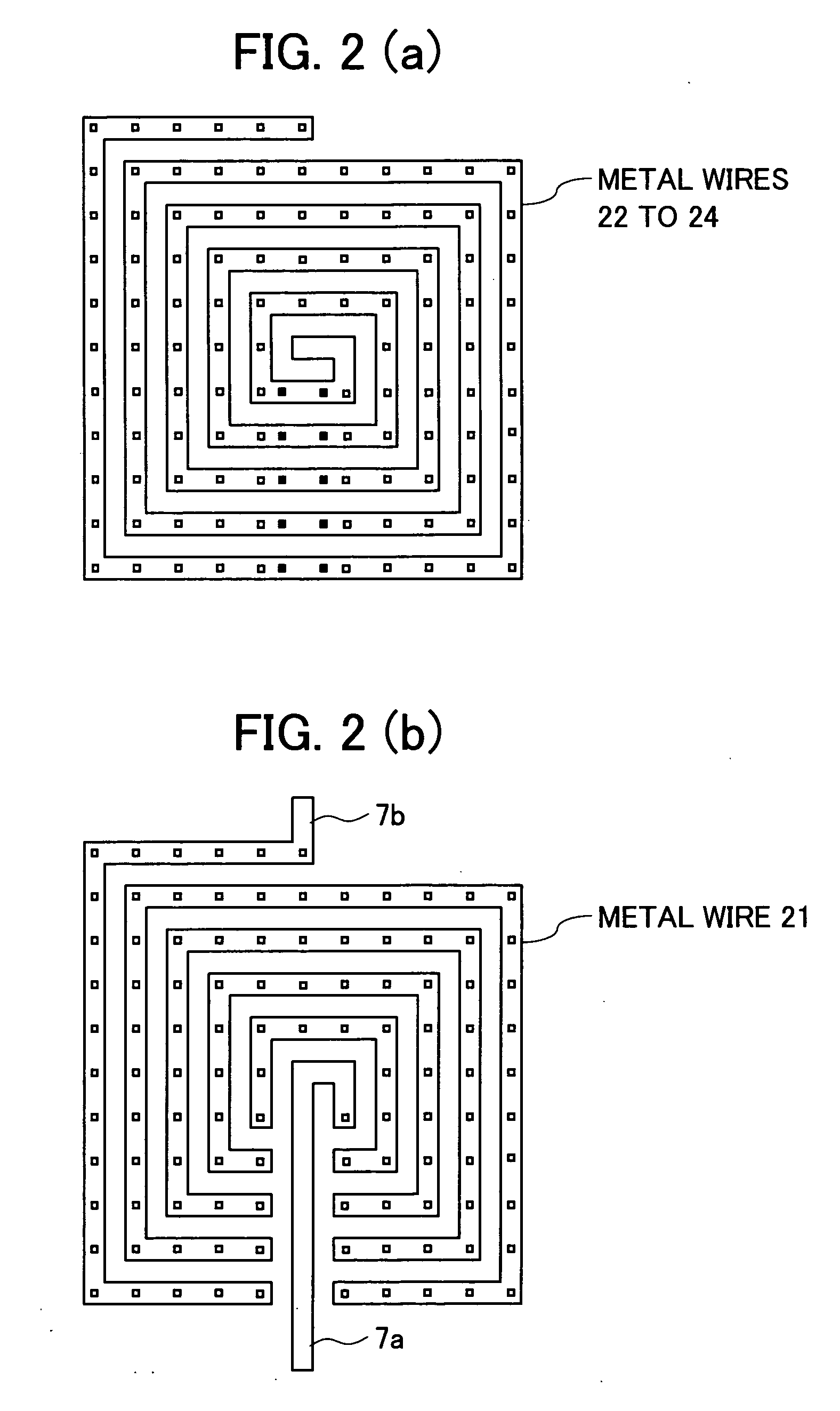
[0042] With reference to FIGS. 1 through 17, one embodiment of the present invention is described below. FIG. 1 is a cross-sectional perspective view illustrating a structure of an inductor of the present invention. FIGS. 2(a) and 2(b) are plan views illustrating patterns of metal wires in the inductor illustrated in FIG. 1.

[0043] As illustrated in FIG. 1, an inductor 1 of the present invention includes first to fourth insulating layers 11 to 14, first to fourth metal wires 21 to 24, and first to third via holes 31 to 33.

[0044] The first to fourth insulating layers 11 to 14 are stacked on a semiconductor substrate (not shown) in the order illustrated in FIG. 1. The first metal wire 21 is formed on an upper surface of the first insulating layer 11 (a surface on the opposite side of the semiconductor substrate), and the second metal wire 22 is formed on an upper surface of the second insulating layer 12. Further, the third metal wire 23 is formed on an upper surface of the third ins...


PUM

PropertyMeasurementUnit
resistanceaaaaaaaaaa

Abstract

An inductor of the present invention includes a plurality of insulating layers being stacked and coil patterns respectively provided on predetermined layers of the insulating layers. The coil patterns are provided on at least two of the insulating layers, and electrically connected to each other. With this arrangement, it is possible to improve Q of the inductor without increasing the size of the inductor.

Description

[0001] This Nonprovisional application claims priority under 35 U.S.C. § 119(a) on Patent Application No. 358975 / 2004 filed in Japan on Dec. 10, 2004, the entire contents of which are hereby incorporated by reference. FIELD OF THE INVENTION [0002] The present invention relates to (i) a spiral inductor which is constructed by a manufacturing process of a semiconductor device, (ii) a resonator and an oscillator both of which include the spiral inductor (e.g. voltage controlled resonant circuit), and (iii) a communication apparatus (e.g. wireless apparatus, high-frequency transmitting and receiving apparatus), (iv) and the like. BACKGROUND OF THE INVENTION [0003] Voltage controlled oscillating circuits are used as local oscillation sources in tuners for satellite broadcasts or tuners for cable television broadcasts. The voltage controlled oscillating circuit includes a resonant circuit having a variable capacitance device, and a negative resistance circuit section having an active comp...

Claims


Application Information

Patent Timeline
Patent Type & Authority Applications(United States)
IPC IPC(8): H01F5/00
CPCH01F17/0013H03B5/1841
Inventor TAMATA, MITSURUHAMAGUCHI, MUTSUMI
Owner SHARP KK
Why Eureka
Try Eureka