Floorplan visualization method

a floorplan and visualization technology, applied in the field of very large scale integrated circuit design technology, can solve the problems of difficult visualization for designers, especially novices, difficult to recognize bad assignments, and conventional solutions are unacceptable, and achieve the effects of convenient implementation, fast and easy analysis, and easy implementation

Active Publication Date: 2006-06-15
BELL SEMICON LLC
View PDF1 Cites 10 Cited by
  • Summary
  • Abstract
  • Description
  • Claims
  • Application Information

AI Technical Summary

Benefits of technology

[0007] The objects, features and advantages of the present invention include providing a floor plan visualization method and / or design tool that may (i) allow placement analysis and visualization, (ii) help with selection of programmable devices, (iii) facilitate IO assignment, diffused memory assignment and R-cell memory placement, (iv) provide a fast and easy analysis, (v) allow evaluation of more permutations than would be possible with a full layout tool, (iv) allow layout analysis very early in a design flow, (vii) be easily implemented and / or (viii) provide a low cost, or no cost, addition to existing design tools.

Problems solved by technology

It is difficult for a designer, especially a novice one, to visualize how big each subsystem is in order to judge the optimum location and allocation for the subsystems.
A bad assignment can be difficult to recognize because the effects are subtle (e.g., bad timing paths, congestion, etc.) and not always distinguishable from non-placement related issues.
The conventional solutions are unacceptable for two reasons.
Relying on the designer to use experience and design knowledge to place and assign subsystems is not desirable because the engineer, even with expertise, can easily mis-estimate the layout and obtain sub-optimal results without being able to identify that the IO and memory allocation / placement played a role.
Performing a full floorplanning analysis with actual netlist data and actual cell area data is only practical for application specific integrated circuit (ASIC) designs where a great deal of time is available to do full floorplanning.
Also, the full floorplanning tools are very expensive and slow.
For designs involving programmable platform devices, a full floorplanning analysis is not practical because the floorplanning tools can cost many times more than the entire engineering costs for the designs.

Method used


Image

  • Floorplan visualization method
  • Floorplan visualization method
  • Floorplan visualization method

Examples


Embodiment Construction

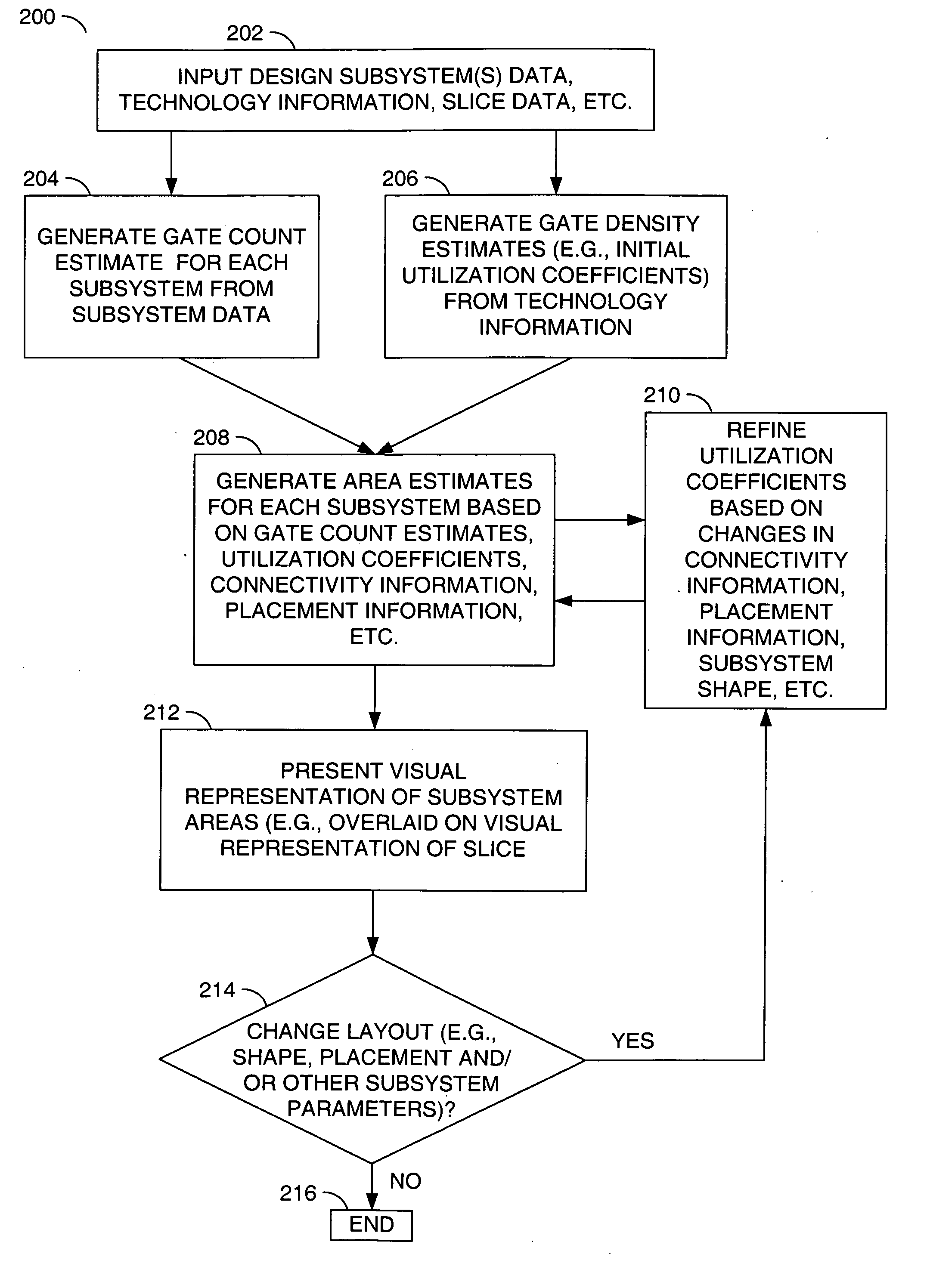
[0014] Referring to FIG. 1, a block diagram of a programmable platform device (or die, or slice) 100 is shown in accordance with a preferred embodiment of the present invention. The slice 100 may be implemented, in one example, as a partially manufactured semiconductor device in which all of the silicon layers have been fabricated and customization may be performed via one or more metal layers. In one example, the slice 100 may comprise one or more regions of diffused memory 102, one or more regions of R-cell memory 104, one or more IP (intellectual property) blocks 106 and a diffused region 108. In another example, multiple diffused regions 108 may be implemented. The regions 102, 104, 106, and 108 may be distributed around the slice 100. The diffused memory 102 and hard (diffused) IP 106 regions are generally fixed. Other blocks (e.g., PLLs, IOs, etc.) may be implemented in a slice to meet the design criteria of a particular application.

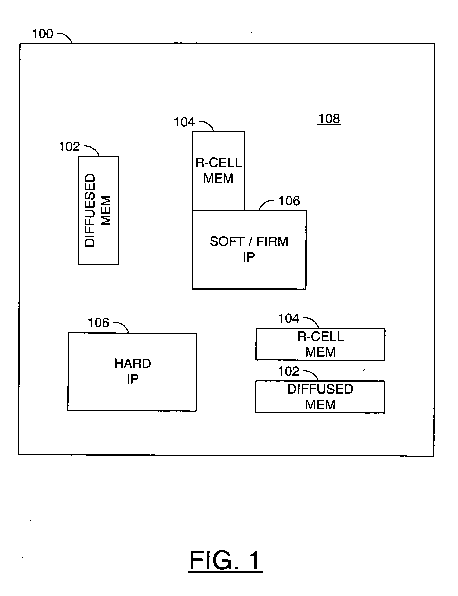
[0015] In one example, a number of slices 1...


PUM


Abstract

A method for floorplan visualization comprising the steps of (A) receiving design information for an integrated circuit design comprising one or more subsystems, (B) generating one or more gate count estimates for the one or more subsystems of the integrated circuit design, (C) generating one or more gate density estimates for gates of the one or more subsystems mapped to one or more programmable areas of a programmable platform device and (D) generating a visual representation of one or more area estimations for each of the one or more subsystems based on the one or more gate count estimates and the one or more gate density estimates.

Description

FIELD OF THE INVENTION [0001] The present invention relates to Very Large Scale Integrated (VLSI) circuit design technology generally and, more particularly, to a floorplan visualization method and / or tool. BACKGROUND OF THE INVENTION [0002] High-level analysis of physical design planning covers the allocation of input / outputs (IOs), diffused memories and location of R-cell memories within integrated circuit designs based on programmable platform devices, such as platform and structured application specific integrated circuits (ASICs). In a conventional design flow a designer decides: (i) where to place IOs, (ii) how to assign functional memories to diffused memories, and (iii) where to place R-cell memories. The decisions are made without the designer being able to see the various subsystems (blocks) and memory topology of the design. The designer typically guesses (or estimates) a size for each subsystem. Assignment and placement decisions are made based on the guess / estimate of t...

Claims


Application Information

Patent Timeline
Patent Type & Authority Applications(United States)
IPC IPC(8): G06F9/455G06F9/45G06F17/50
CPCG06F17/5072G06F30/392
Inventor MARTIN, GREGOR J.HE, YING CHUNLINDBERG, GRANT
Owner BELL SEMICON LLC
Why Eureka
Try Eureka