Wafer-scale microcolumn array using low temperature co-fired ceramic substrate

a co-fired ceramic and micro-column array technology, applied in the direction of material analysis using wave/particle radiation, instruments, nuclear engineering, etc., can solve the problems of too complicated manufacturing process and high cost, and achieve the effect of simple process and low cos

a co-fired ceramic and micro-column array technology, applied in the direction of material analysis using wave/particle radiation, instruments, nuclear engineering, etc., can solve the problems of too complicated manufacturing process and high cost, and achieve the effect of simple process and low cos

US20060131698A1Inactive Publication Date: 2006-06-22ELECTRONICS & TELECOMM RES INST +1

Image

  • Wafer-scale microcolumn array using low temperature co-fired ceramic substrate
  • Wafer-scale microcolumn array using low temperature co-fired ceramic substrate
  • Wafer-scale microcolumn array using low temperature co-fired ceramic substrate

Examples


Embodiment Construction

[0022] The present invention will now be described more fully with reference to the accompanying drawings in which embodiments of the invention are shown. The invention may, however, be embodied in many different forms and should not be construed as being limited to the embodiments set forth herein; rather, these embodiments are provided so that this disclosure will be thorough and complete, and will fully convey the concept of the invention to those skilled in the art.

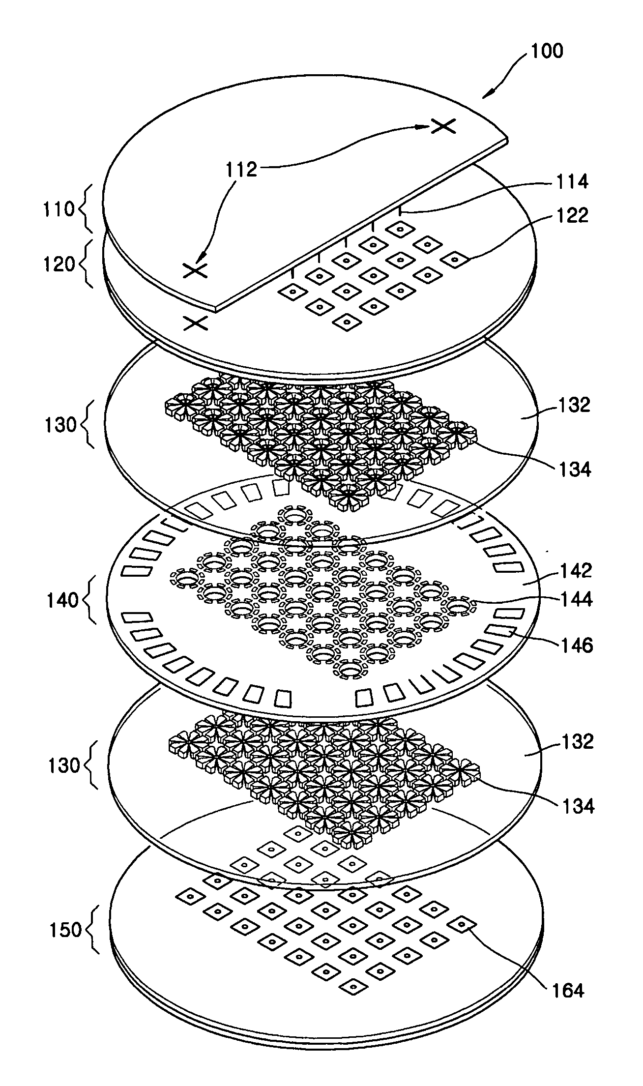
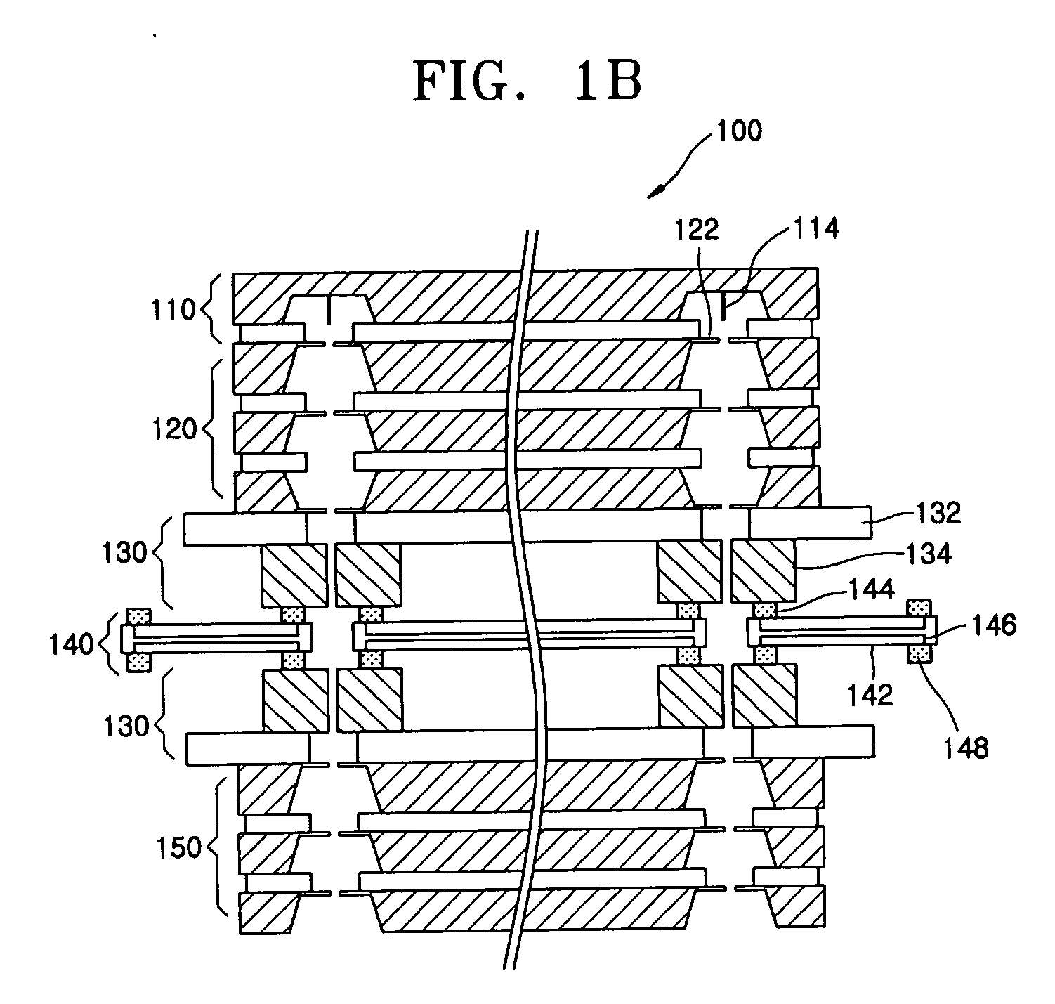
[0023]FIG. 1A is an exploded perspective view of a wafer-scale microcolumn array 100 according to an embodiment of the present invention, and FIG. 1B is a schematic cross-sectional view of FIG. 1A.

[0024] Referring to FIGS. 1A and 1B, when the wafer-scale microcolumn array 100 is formed, wirings between a beam deflector array 130 and electron lens arrays 120 and 150 must be integrated into small spaces. Although use of typical semiconductor process technologies can satisfy this demand, in the case of wirings of a mul...


PUM

PropertyMeasurementUnit
electric conductivityaaaaaaaaaa
conductiveaaaaaaaaaa
voltageaaaaaaaaaa

Abstract

Provided is a wafer-scale microcolumn array using a low temperature co-fired ceramic (LTCC) substrate. The microcolumn array includes a LTCC substrate having wirings and wafer-scale beam deflector arrays, which are attached to at least one side of the LTCC substrate and has an array of deflection devices deflecting electron beams. The wafer-scale microcolumn array using the LTCC substrate makes it possible to significantly increase the throughput of semiconductor wafers, simplify its manufacturing process, and lower its production cost.

Description

CROSS-REFERENCE TO RELATED PATENT APPLICATION [0001] This application claims the benefit of Korean Patent Application Nos. 10-2004-0109002, filed on Dec. 20, 2004 and 10-2005-0051981, filed on Jun. 16, 2005, in the Korean Intellectual Property Office, the disclosures of which are incorporated herein in their entirety by reference. BACKGROUND OF THE INVENTION [0002] 1. Field of the Invention [0003] The present invention relates to an apparatus used in electron beam lithography, and more particularly, to a wafer-scale microcolumn array using a low temperature co-fired ceramic (LTCC) substrate. [0004] 2. Description of the Related Art [0005] An electron beam microcolumn (hereinafter, referred to as a microcolumn) used for minutely focusing an electron beam was first introduced at the end of the 1980s. The microcolumn has advantages of small size, high resolution, and low production cost. The microcolumn has been applied to various fields, such as electron beam lithography, etc. [0006] ...

Claims


Application Information

Patent Timeline
22 Jun 2006
Publication
US20060131698A1
IPC
H01L23/544
CPC
B82Y10/00; B82Y40/00; H01J37/04; H01J37/3177; H01J2237/0492; H01J2237/1205; H01J2237/1518
Inventors
JEONG, JIN WOO; KIM, DAE JUN