Method and apparatus for clamping a substrate in a high pressure processing system

Inactive Publication Date: 2006-06-22
TOKYO ELECTRON LTD
View PDF99 Cites 18 Cited by
  • Summary
  • Abstract
  • Description
  • Claims
  • Application Information

AI Technical Summary

Benefits of technology

[0015] According to certain principles of the present invention, a processing system is provided which comprises a processing chamber configured to treat said substrate therein with a high pressure fluid; a platen coupled to said processing chamber and configured to support said substrate, a fluid supply system, a fluid flow system coupled to said fluid supply system and said chamber and c

Problems solved by technology

Moreover, the advent of new materials, such as low dielectric constant (low-k) materials, limits the use of plasma ashing due to their susceptibility to damage during plasma exposure.
Certain challenges occur when attempting to process silicon wafers under high pressure.
One such issue is how to hold the wafer in place during processing.
In such a case, bias in pressure keeps the wafer in place during processing, which may include violent events such as sudden decompressions, high surface velocity jets for cleaning, etc.
One of the significant drawbacks of vacuum holding is the restraining of the wafer against the platen.
If a wafer is held against a platen, typically of stainless steel, the resulting static pressure load can force the wafer against the platen, which can cause damage to the backside of the wafer.
This can cause irreparable harm to the wafer for subsequent process steps.
The wafer may or may not be able to follow the new shape that the pl

Method used


Image

  • Method and apparatus for clamping a substrate in a high pressure processing system
  • Method and apparatus for clamping a substrate in a high pressure processing system
  • Method and apparatus for clamping a substrate in a high pressure processing system

Examples


Example

[0029] In the following description, to facilitate a thorough understanding of the invention and for purposes of explanation and not limitation, specific details are set forth, such as a particular geometry of the processing system and various descriptions of the system components. However, it should be understood that the invention may be practiced with other embodiments that depart from these specific details.

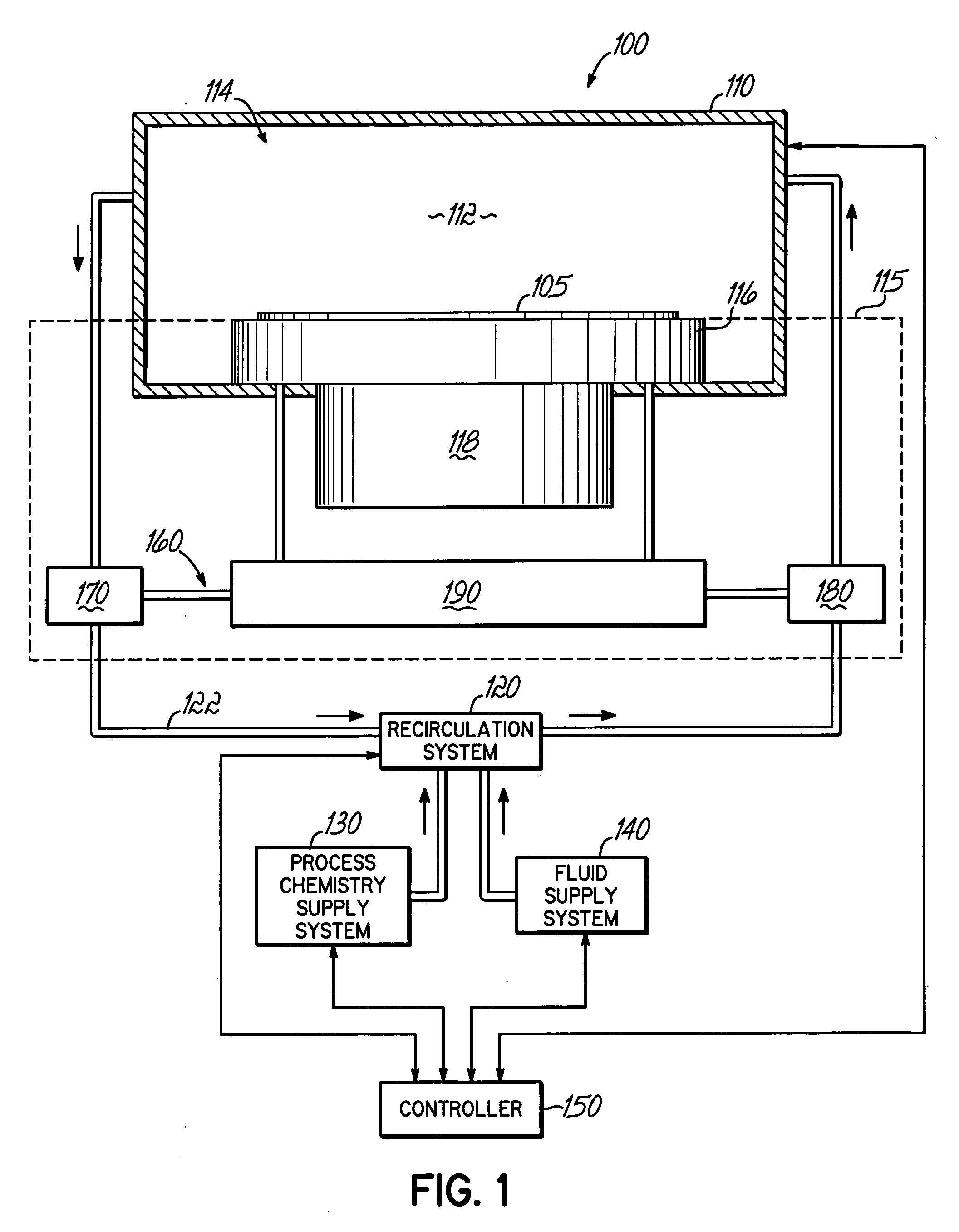
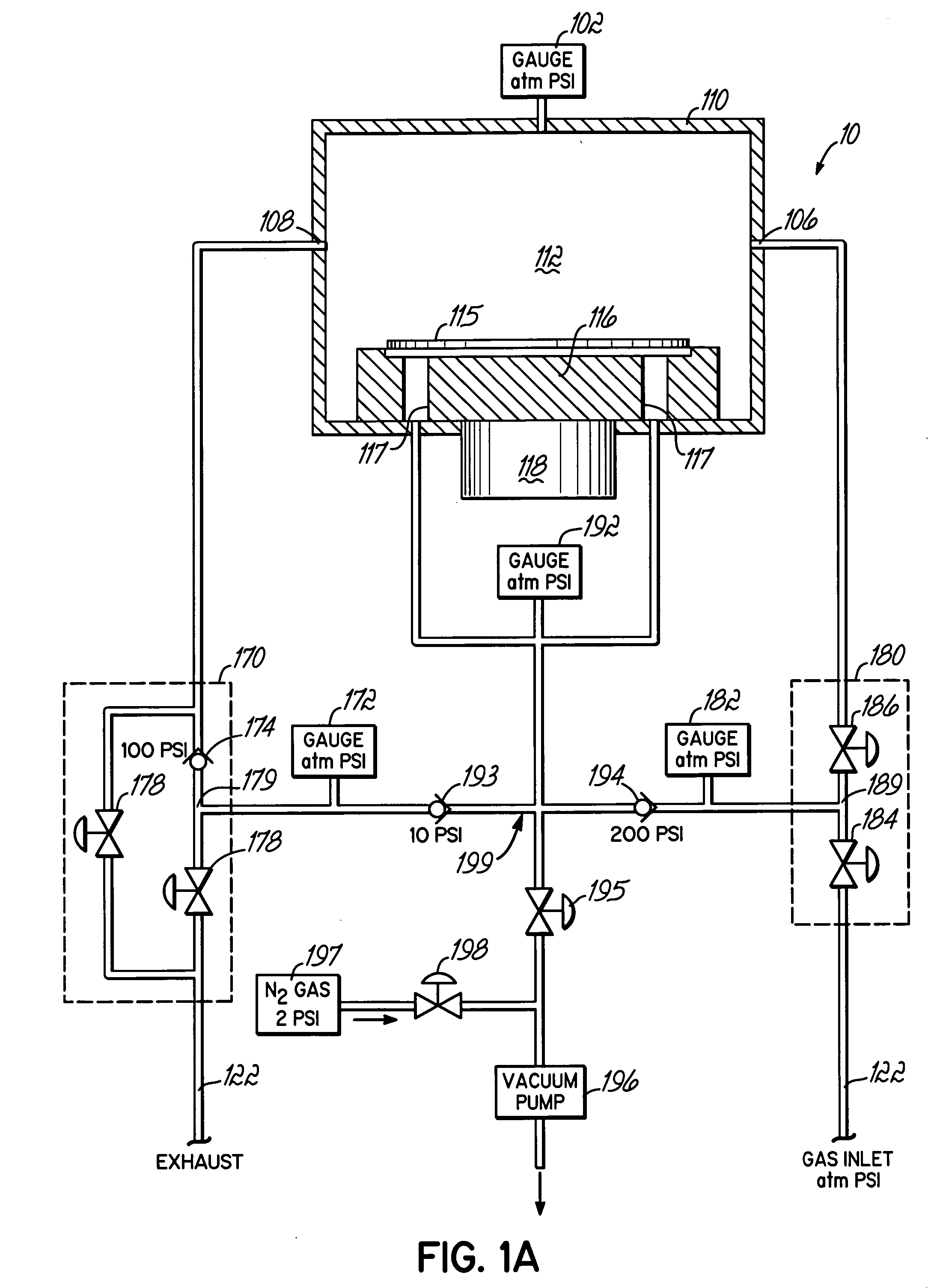
[0030] Referring now to the drawings, wherein like reference numerals designate identical or corresponding parts throughout the several views, FIG. 1 illustrates a processing system 100 according to an embodiment of the invention. In the illustrated embodiment, processing system 100 is configured to treat a substrate 105 with a high pressure fluid, such as a fluid in a supercritical state, with or without other additives, such as process chemistry. The processing system 100 comprises processing elements that include a processing chamber 110, a fluid flow system 120, a proces...


PUM

PropertyMeasurementUnit
Pressureaaaaaaaaaa
Pressureaaaaaaaaaa
Temperatureaaaaaaaaaa

Abstract

Pressure biased wafer holding of a semiconductor wafer is provided for use in high pressure processing. The use of vacuum chucking for holding a semiconductor wafer during processing is applied to high pressure systems. Adverse effects of high pressure biases are prevented by a valve arrangement that reduces or limits the holding load on a wafer. Check valves and on-off valves connected to input and output lines to the chamber bias fluid applied to a wafer supporting platen to vary the backside pressure so that the excess of frontside pressure versus backside pressure on the wafer is kept within an effective clamping range without excessive force being applied to the wafer. Use of fluid-mechanical techniques is maximized in certain described embodiments to avoid disadvantages of electronic control systems.

Description

FIELD OF THE INVENTION [0001] The present invention relates to a method and system for clamping a substrate in a high pressure processing system and, more particularly, in a supercritical processing system. BACKGROUND OF THE INVENTION [0002] During the fabrication of semiconductor devices for integrated circuits (ICs), a sequence of material processing steps, including both pattern etching and deposition processes, are performed, whereby material is removed from or added to a substrate surface, respectively. During, for instance, pattern etching, a pattern formed in a mask layer of radiation-sensitive material, such as photoresist, using for example photolithography, is transferred to an underlying thin material film using a combination of physical and chemical processes to facilitate the selective removal of the underlying material film relative to the mask layer. [0003] Thereafter, the remaining radiation-sensitive material, or photoresist, and post-etch residue, such as hardened ...

Claims


Application Information

Patent Timeline
IPC IPC(8): B24B7/30B24B29/00B24B47/00
CPCH01L21/02101H01L21/67057H01L21/6838
Inventor SHEYDAYI, ALEXEI
Owner TOKYO ELECTRON LTD
Why Eureka
Try Eureka