Semiconductor device fabrication method

a technology of semiconductor devices and fabrication methods, applied in the direction of photomechanical equipment, instruments, originals for photomechanical treatment, etc., can solve the problems of long processing time, long lift-off time, long processing time, etc., and achieve the effect of reducing the length of lift-off processing time, facilitating lift-off, and ensuring the accuracy of metal patterns

Inactive Publication Date: 2006-06-29
HITACHI CABLE
View PDF4 Cites 6 Cited by
  • Summary
  • Abstract
  • Description
  • Claims
  • Application Information

AI Technical Summary

Benefits of technology

[0032] According to the present invention, because of no sidewall deposition layer joined to the metal pattern, lift-off can be facilitated, allowing the length of time for lift-off processing to be greatly reduced. Also, no burrs are caused to the finished metal pattern at all and in addition, regarding precision for the metal pattern, even in the case of a micro metal pattern, by facilitating controlling the resist cross-sectional shape according to the tendency of deposition metal particles to diffract, a high-precision pattern can be formed

Problems solved by technology

Because the cross-section of the positive type resist layer 43 typically used is in a not vertical but slightly forward tapered shape, however, making the metal film 45 thick also makes the sidewall deposition layer 45s thick, which causes difficulty in lift-off, and consequently makes the length of time for the processing long.
As a consequence, there is the problem that a wiring short-circuiting or multilayer wiring disconnection or short-circuiting takes place.
In these methods, however, there is the problem of a drop in precision for resist patterning.
As illustrated in FIG. 2C, on the other hand, there is the method for forming the cross-section of a resist layer 71 in a vertical or inverse tapered shape, by image inversion of a positive type resist layer into a negative type resist layer, and subsequent development, which however also poses the problems with the vertical pattern having little effect on making the sidewall deposition layer 45s thin, or with the inverse tapered shape having to intentionally reduce resolution for resist patterning, and making the shape uncontrollable.
Because the semiconductor device fabrication method described in Japanese patent No. 3339331 forms the surface resist layer in a forward tapered shape, however, there is a limit on adaptation to a micro metal pattern that serves as electrodes and wiring of the semiconductor device, and it is difficult to ensure precision for micro metal pattern shape, which is because, generally, in forward tapered shapes, precision for tapered shapes has a larger effect on the precision for metal pattern shape subsequently formed than in inverse tapered shapes.

Method used


Image

  • Semiconductor device fabrication method
  • Semiconductor device fabrication method
  • Semiconductor device fabrication method

Examples


Embodiment Construction

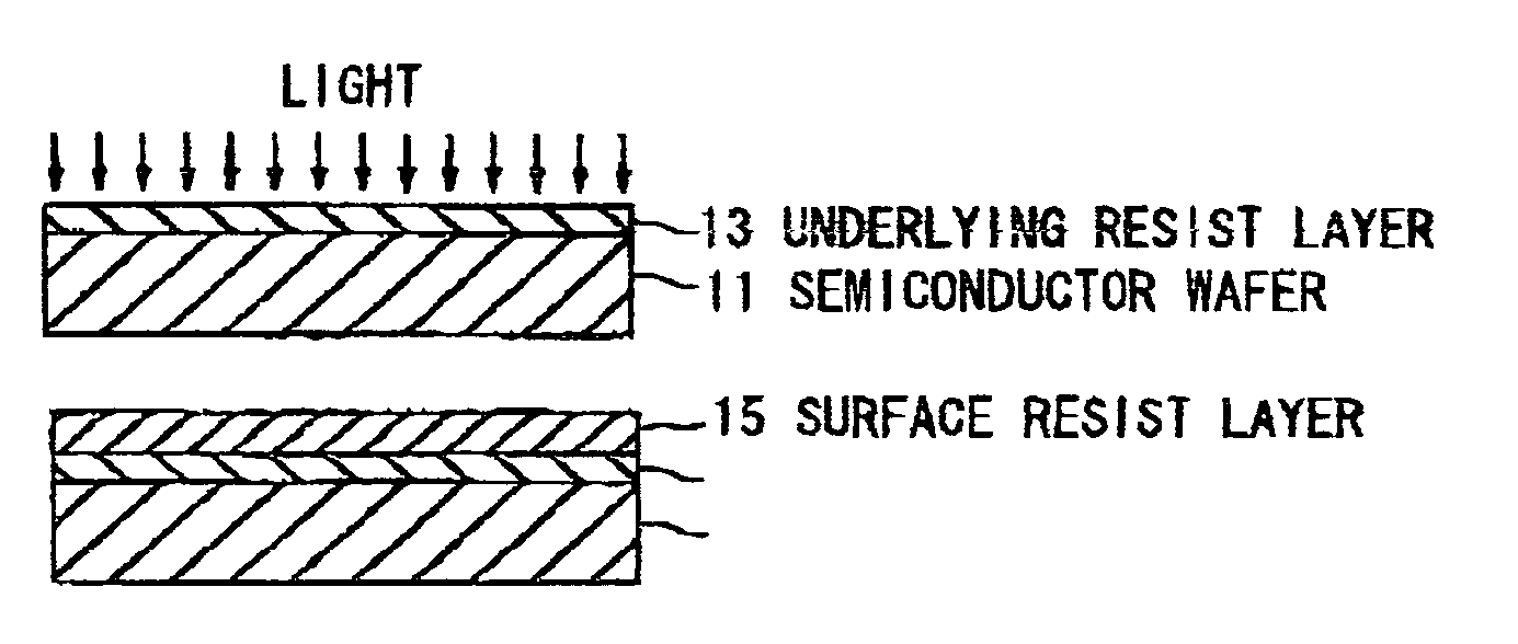
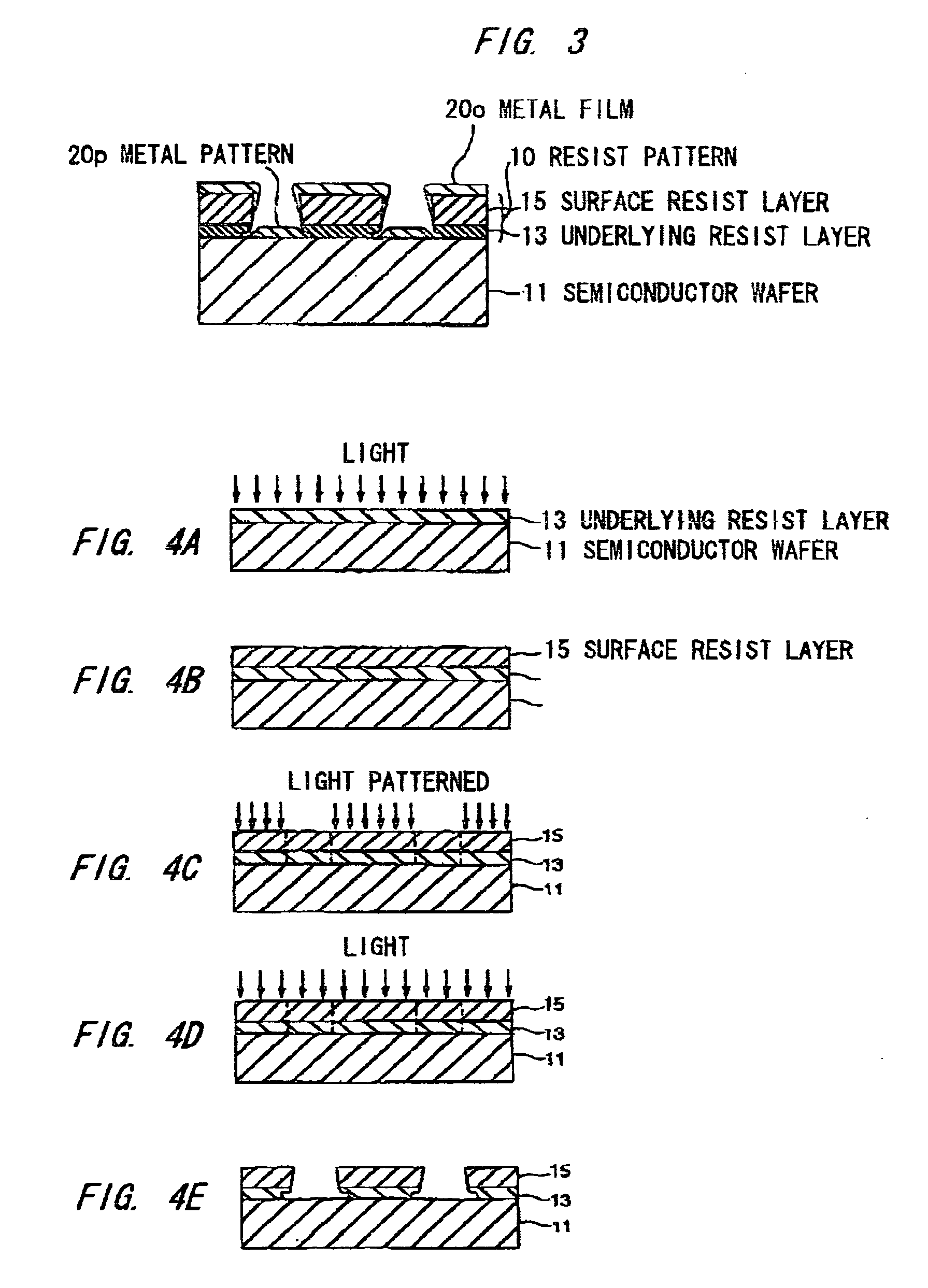
[0041]FIGS. 4A-4E illustrate a fabrication process for a resist pattern in the present embodiment.

[0042] First, as illustrated in FIG. 4A, on a semiconductor wafer 11 is formed a diazo novolac positive type photoresist with a film thickness of 1.5-2.5 μm, followed by light exposure of its entire surface, according to needs, to form an underlying resist layer 13. The conditions for this light exposure of entire surface are important in controlling mutual diffusion of resist layer 13 and subsequently-formed surface resist layer 15 often used in an image inversion technique, and the like, as will be explained later.

[0043] Next, as illustrated in FIG. 4B, there is formed a surface resist layer 15 with a film thickness of 2.5-3.5 μm, which is often used in the above-mentioned image inversion technique, and the like. In comparison to typical diazo novolac positive type photoresists, the positive type photoresist for this surface resist layer 15 is inverted into a negative type by only l...


PUM

PropertyMeasurementUnit
dissolvingaaaaaaaaaa
physical forceaaaaaaaaaa
lengthaaaaaaaaaa

Abstract

A semiconductor device fabrication method applies a diazo novolac photoresist to a semiconductor wafer, followed by light exposure of its entire surface to form an underlying resist layer; forms a surface resist layer thereover; performs patterned-light exposure and heat treatment to the photoresist film consisting of the two resist layers formed; and exposes its entire surface to light, followed by development to process the photoresist film into a resist pattern, where the surface resist layer is in an inverse tapered shape, while the underlying resist layer is in an undercut shape relative to the surface resist layer.

Description

[0001] The present application is based on Japanese patent application Nos. 2004-185544 and 2005-131009, the entire contents of which are incorporated herein by reference. BACKGROUND OF THE INVENTION [0002] 1. Field of the Invention [0003] This invention relates to a semiconductor device fabrication method involving the step of lift-off patterning of a metal film for forming electrodes and wiring. [0004] 2. Description of the Related Art [0005] As a patterning method for electrodes and wiring of semiconductor devices, lift-off processing is used in many cases, in which, as illustrated in FIG. 1A, a resist layer 43 is formed on a semiconductor wafer 41 as a mask, followed by vacuum deposition of a metal film 45 on the resist layer 43, and subsequent immersion thereof in an organic solvent such as acetone or the like to remove the resist layer 43 and the metal film 45 formed thereon. [0006] In this lift-off patterning, a thin sidewall deposition layer 45s is formed on a sidewall of th...

Claims


Application Information

Patent Timeline
Patent Type & Authority Applications(United States)
IPC IPC(8): H01B13/00C23F1/00G03F1/00C03C25/68G03F7/26H01L21/027H01L21/28H01L21/306H01L21/3205H01L21/768
CPCC23F1/02G03F1/36G03F7/095G03F7/2022G03F7/70433H01L21/28506H01L21/32051
Inventor KOIZUMI, GENTA
Owner HITACHI CABLE
Why Eureka
Try Eureka