Method of nano thin film thickness measurement by auger electron spectroscopy

a thin film and electron spectroscopy technology, applied in the field of thin films, can solve the problems of complex sample preparation, limited application of afm, and measurement of thickness

Active Publication Date: 2006-06-29
SAE MAGNETICS (HK) LTD
View PDF9 Cites 38 Cited by
  • Summary
  • Abstract
  • Description
  • Claims
  • Application Information

AI Technical Summary

Problems solved by technology

The disadvantage of AFM is that it requires elaborate sample preparation and can only measure the thickness of a mono-layer or the combined total thickness of a multi-layer film.
Therefore, the usefulness of AFM is limited to calibration applications.
However, this method requires complicated and time-consuming sample preparation by a Focus Ion Beam (FIB), to create a cross section and, then, measuring the thickness by TEM.
Such a “destructive” measurement is unde

Method used


Image

  • Method of nano thin film thickness measurement by auger electron spectroscopy
  • Method of nano thin film thickness measurement by auger electron spectroscopy
  • Method of nano thin film thickness measurement by auger electron spectroscopy

Examples


Embodiment Construction

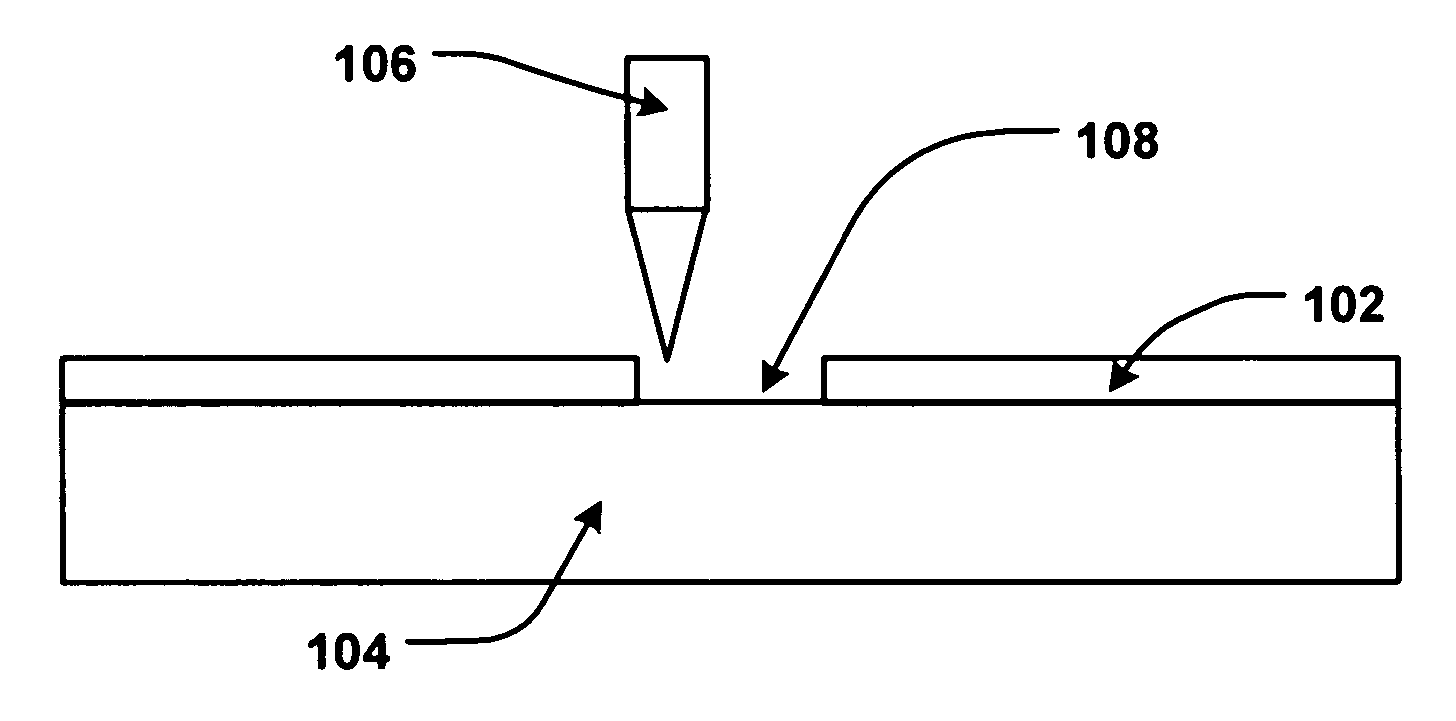
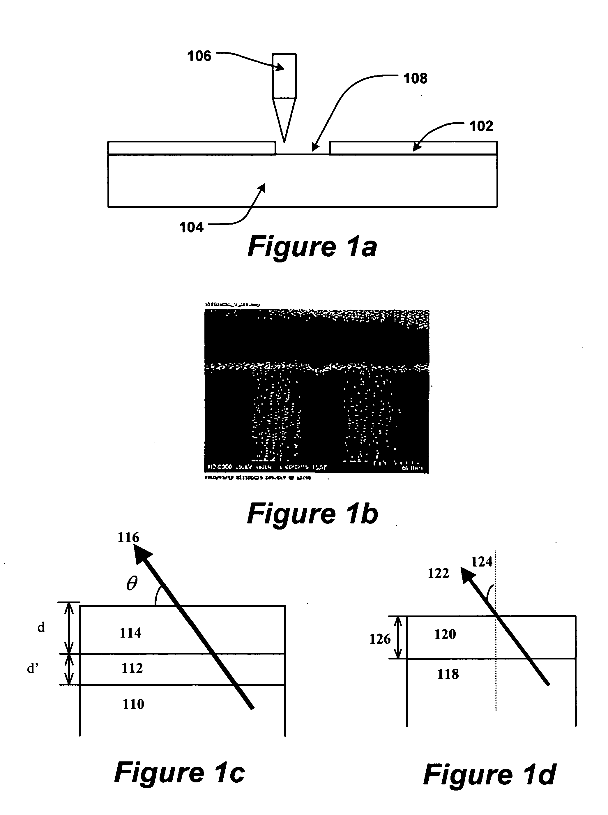
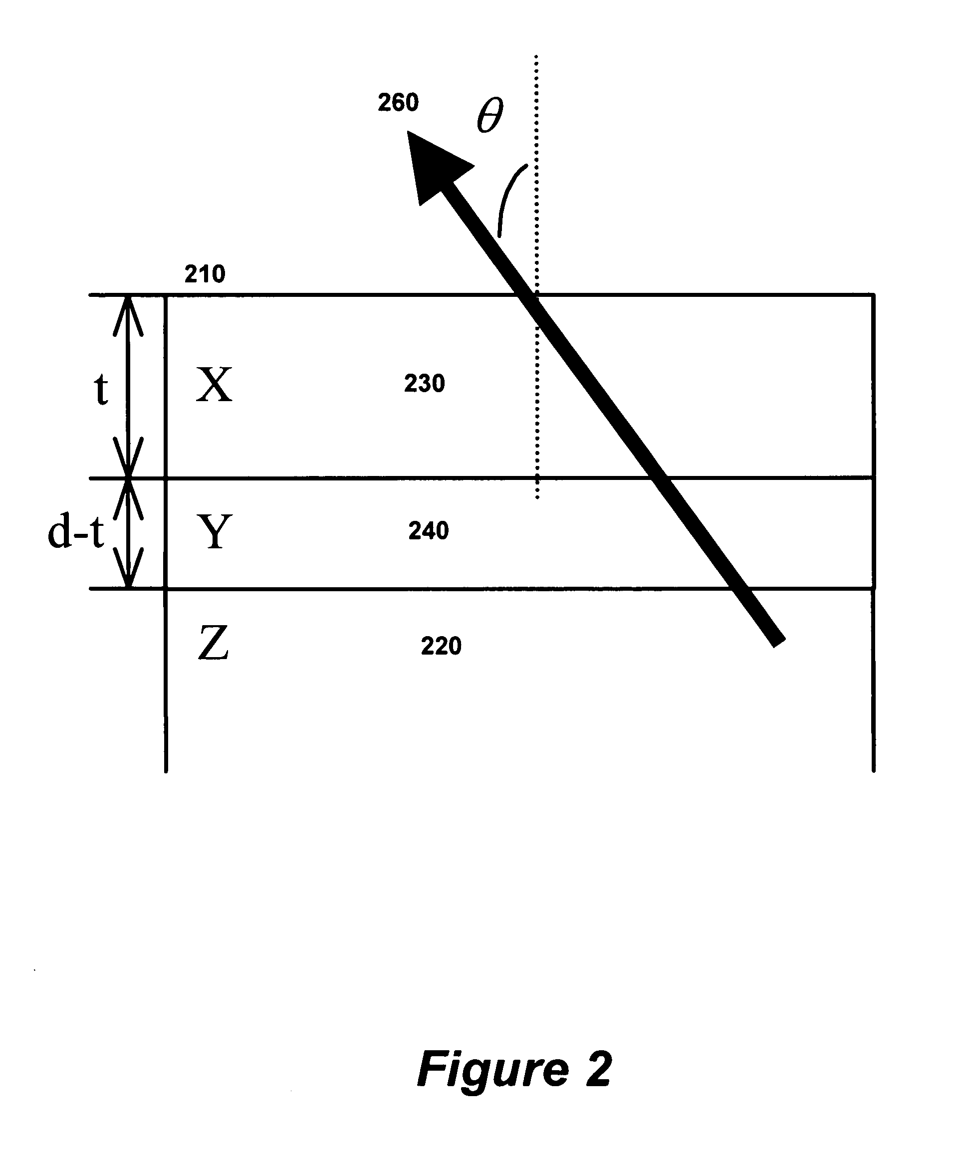
[0014] A system and method for measuring the thickness of an ultra-thin multi-layer film structure on a substrate is disclosed. A physical model of an Auger emission from a nano multilayer structure is built. A mathematical model of Auger electron spectroscopy (AES) measurement of ultra-thin film thickness is derived according to the physical model. By performing the AES measurements on a series of calibration samples, the parameters in the mathematical model are determined. The parameters may be calibrated by comparing the results to the results from correlation measurement by alternative techniques, such as transmission electron microscope (TEM), atomic force microscope (AFM), and electron spectroscopy for chemical analysis (ESCA), establishing a physical model. AES analysis is performed on the practical samples to measure the signal intensity of the related elements in the ultra-thin multi-layer film structure. The results are input into the mathematical model and the thickness i...


PUM


Abstract

A system and method for measuring the thickness of an ultra-thin multi-layer film on a substrate is disclosed. A physical model of an ultra-thin multilayer structure and Auger electron emission from the nano-multilayer structure is built. A mathematical model for the Auger Electron Spectroscopy (AES) measurement of the multilayer thin film thickness is derived according to the physical model. Auger electron spectroscopy (AES) is first performed on a series of calibration samples. The results are entered into the mathematical model to determine the parameters in the mathematical equation. The parameters may be calibrated by the correlation measurements of the alternate techniques. AES analysis is performed on the ultra-thin multi-layer film structure. The results are entered into the mathematical model and the thickness is calculated.

Description

BACKGROUND INFORMATION [0001] The present invention relates to thin-films on substrates. Specifically, the present invention relates to the use of Auger Electron Spectroscopy in the measurement of the thickness of an ultra-thin film on a substrate. [0002] Ultra-thin films with thickness of less than five nanometers have found increasing application in the development of nano-technology. The exact thickness of such ultra-thin film is important for both the basic studies of multi-layer nano-structures and in the technical specifications of nano-device fabrication. For example, in the production of a magnetic head for a hard disc drive (HDD); an ultra-thin diamond-like-carbon (DLC) film is coated on the slider substrate, with an ultra-thin silicon (Si) film as the transition layer in between, to protect the writer / reader sensor. With the rapid increase of the HDD recording density to 80 G bits / inch2, the flying height of the slider over the disc has been reduced to about 10 nm. Corresp...

Claims


Application Information

Patent Timeline
IPC IPC(8): G21K7/00G01N23/00
CPCG01B15/02G01N23/2276
Inventor JIANG, ZHI CHENGLI, SHAN DANKAM, YUEN KWANLIU, YI WEI
Owner SAE MAGNETICS (HK) LTD
Why Eureka
Try Eureka