Semiconductor photoelectric surface and its manufacturing method, and photodetecting tube using semiconductor photoelectric surface

a semiconductor photoelectric surface and semiconductor technology, applied in the direction of photoelectric discharge tubes, discharge tubes main electrodes, electron multiplier details, etc., can solve the problems of significant reduction in cathode sensitivity or gain, and difficulty in providing a getter using a conventional titanium wire in the vicinity, so as to achieve the effect of miniaturizing the photomultiplier tube and being convenient to install

Inactive Publication Date: 2006-06-29
HAMAMATSU PHOTONICS KK
View PDF2 Cites 10 Cited by
  • Summary
  • Abstract
  • Description
  • Claims
  • Application Information

AI Technical Summary

Benefits of technology

[0008] As a result of this, the metal electrode in film form serves as an ohmic electrode for an electrical connection of the photoelectric surface and for the supply of electrons to the photoelectric surface, and in addition, serves as a getter having an effect of gettering a residual gas due to the activation of titanium that is included in the electrode. Furthermore, the electrode in film form that includes

Problems solved by technology

However, in the case of a compact photomultiplier tube or the like, it is extremely difficult to provide a getter using a conventional titanium wire in the vicinity of the photocathode due to a small inner space.
In particular, in the case where a conventional getter is provided between the pho

Method used


Image

  • Semiconductor photoelectric surface and its manufacturing method, and photodetecting tube using semiconductor photoelectric surface
  • Semiconductor photoelectric surface and its manufacturing method, and photodetecting tube using semiconductor photoelectric surface
  • Semiconductor photoelectric surface and its manufacturing method, and photodetecting tube using semiconductor photoelectric surface

Examples


Embodiment Construction

[0022] A semiconductor photocathode according to an Embodiment of the present invention is described in reference to the drawings. The same symbols are attached to the same parts so that the same descriptions can be omitted in cases where possible.

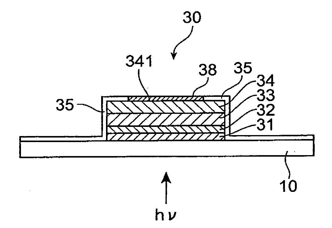
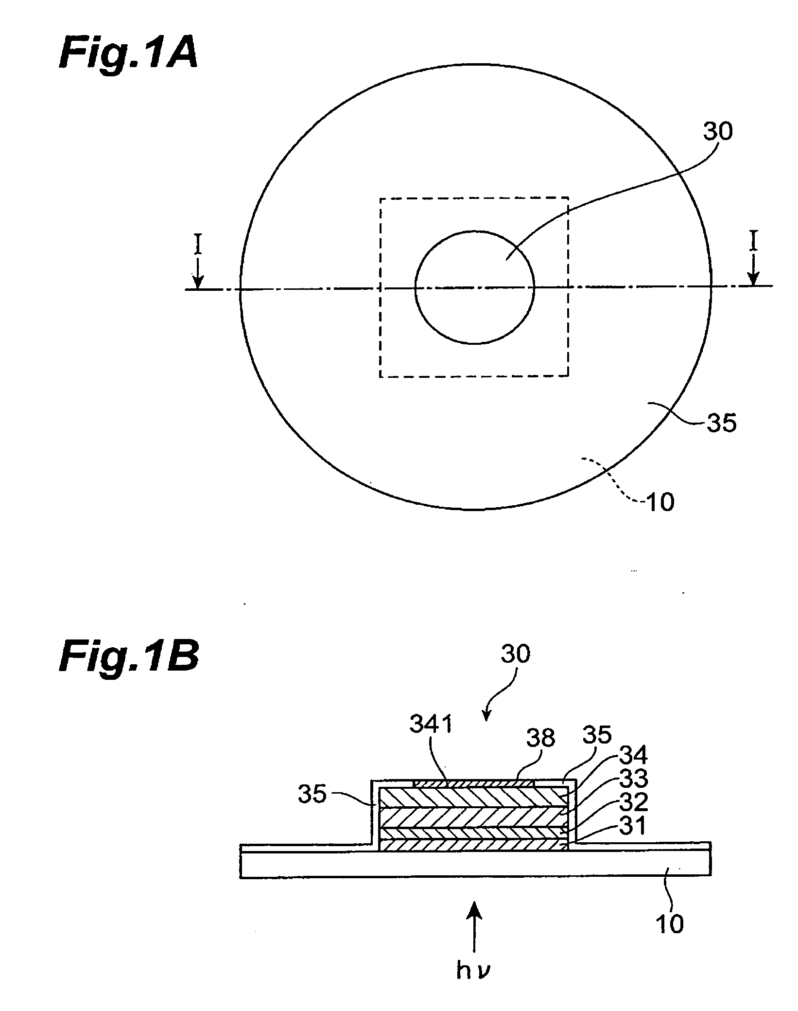
[0023]FIG. 1A is a plan view of a photoelectric surface 30 and a plate of a glass surface 10 as viewed from the vacuum side.

[0024]FIG. 1B is a cross-sectional view along line I-I indicated by arrows of photoelectric surface 30 and the plate of a glass surface 10 shown in FIG. 1A. Here, for the sake of description, the scale of enlargement in the longitudinal direction is greater than the scale of enlargement in the lateral direction in FIG. 1B.

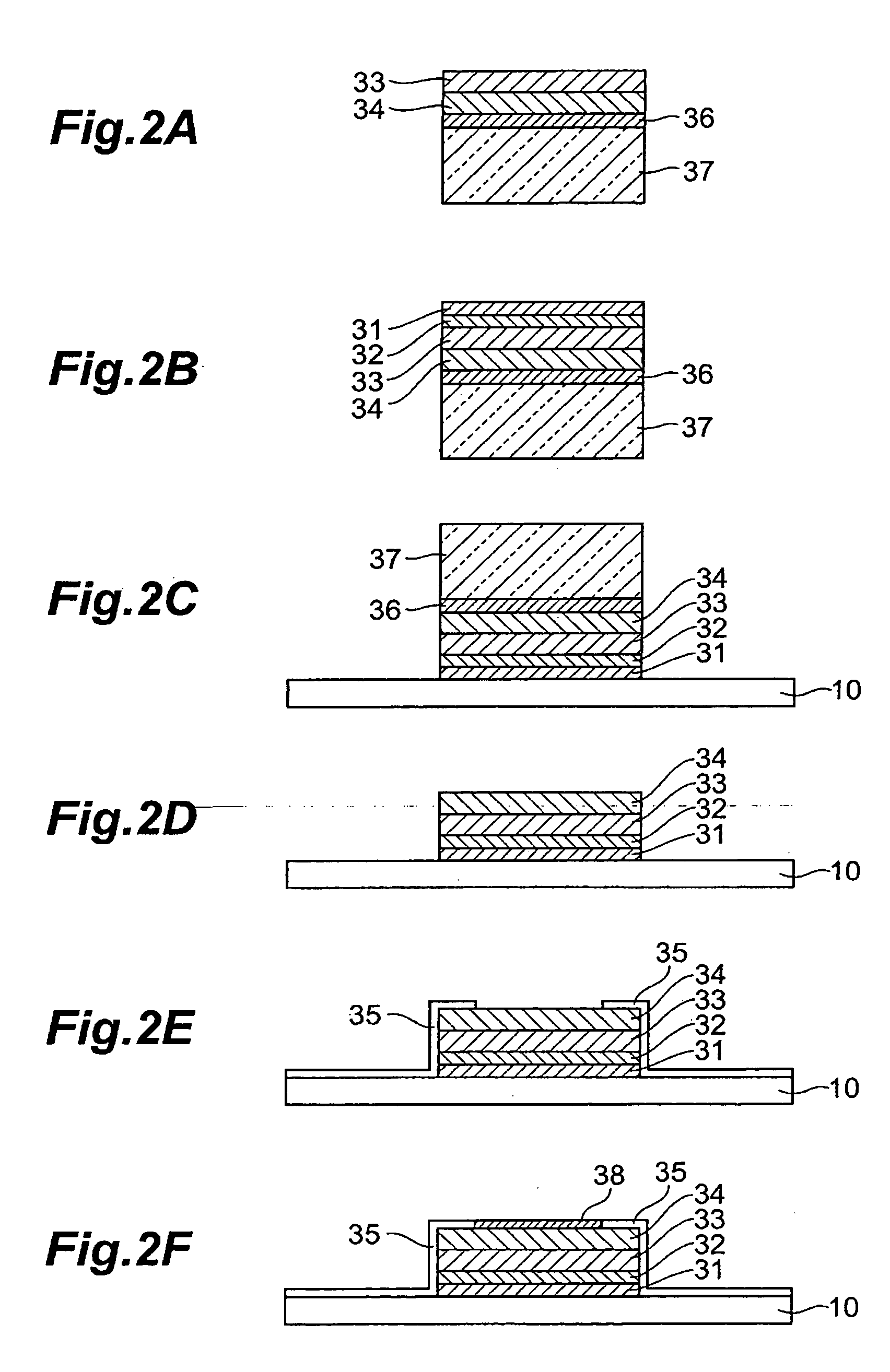
[0025] Light to be detected (hν) enters into photoelectric surface 30 from the lower side of FIG. 1B, wherein the region on the upper side of the photoelectric surface is set to a vacuum condition in FIG. 1B. As shown in FIG. 1B, photoelectric surface 30 is formed by layering a plurality of semico...


PUM


Abstract

A semiconductor photocathode of the present invention is provided with: a support substrate 10; a photoelectric surface 30 which is formed of a plurality of semiconductor layers layered on this support substrate 10 and which emits photoelectrons from a photoelectron emitting surface 341 in response to the incidence of light to be detected; and a metal electrode 35 which is formed in film form so as to coat at least a portion of support substrate 10 and a portion of photoelectric surface 30 and which makes ohmic contact with the photoelectric surface, wherein metal electrode 30 in film form includes titanium and the electron affinity of photoelectron emitting surface 341, which is an exposed portion of photoelectric surface 30 without being coated with metal electrode 35 in film form, is in a negative condition.

Description

TECHNICAL FIELD [0001] The present invention relates to a semiconductor photocathode (NEA semiconductor photocathode) where the electron affinity of the photoelectron emitting surface is in a negative condition and to a manufacturing method for the same as well as to a photodetector tube (a photoelectric tube, a photomultiplier tube or the like) using this semiconductor photocathode. BACKGROUND ART [0002] Residual gas in the vicinity of a photocathode causes noise (after pulse) at the time of measurement in a photodetector tube such as a photomultiplier tube and, therefore, it is important to remove residual gas in the vicinity of the photocathode. In particular, it is very important in a photomultiplier tube to remove residual gas between the photocathode and the first dynode (secondary photomultiplying part), enhancing the vacuum level within the vacuum tube, in order to reduce the after pulse. A method for sputtering a titanium wire within the vacuum tube so as to getter residual...

Claims


Application Information

Patent Timeline
IPC IPC(8): H01L29/06H01J1/34H01J9/12H01J40/06H01J43/08
CPCH01J1/34H01J9/12H01J40/06H01J43/08
Inventor KOHNO, YASUYUKINAGAI, TOSHIMITSUHASEGAWA, YUTAKA
Owner HAMAMATSU PHOTONICS KK
Why Eureka
Try Eureka