Plating apparatus and plating method

a technology of plating apparatus and plating solution, which is applied in the direction of coatings, electrolysis components, electrolysis processes, etc., can solve the problems of increasing the amount, increasing the amount, and likely to produce air bubbles in the plating solution

Inactive Publication Date: 2006-06-29
EBARA CORP
View PDF51 Cites 75 Cited by
  • Summary
  • Abstract
  • Description
  • Claims
  • Application Information

AI Technical Summary

Benefits of technology

[0011] The present invention has been made in view of the above drawbacks. It is, therefore, a first object of the present invention to provide a plating apparatus and a plating method which can introduce a plating solution reliably into an opening in a resist applied on a surface of a substrate without adding any surface-active agent in a plating solution and can achieve a plating process without any plating defects such as insufficient plating.

Problems solved by technology

However, when the surface tension of the plating solution is lowered, air bubbles are likely to be produced in the plating solution when the plating solution is circulated.
Further, when a new surface-active agent is added to a plating solution, anomaly of deposition may occur so as to increase the amount of organic substances trapped in the plated films.
Thus, a surface-active agent may adversely affect properties of the plated films.
Thus, according to a conventional electroplating apparatus using a dipping-type electroplating process, it is difficult to automate an entire plating process from loading of a substrate to unloading of the substrate after a plating process.
However, the conventional plating apparatus for bump formation is designed to perform processes until a plating process, but not to perform processes after the plating process, in consideration of manufacturing lead-time suitable for mass production of a limited variety of goods.
Accordingly, the conventional plating apparatus for bump formation cannot continuously perform a sequence of processes to complete bump formation.
Further, the conventional plating apparatus for bump formation requires a large space for additional process units such as a resist stripping unit and an etching unit and has less flexibility in arrangement.

Method used


Image

  • Plating apparatus and plating method
  • Plating apparatus and plating method
  • Plating apparatus and plating method

Examples


first embodiment

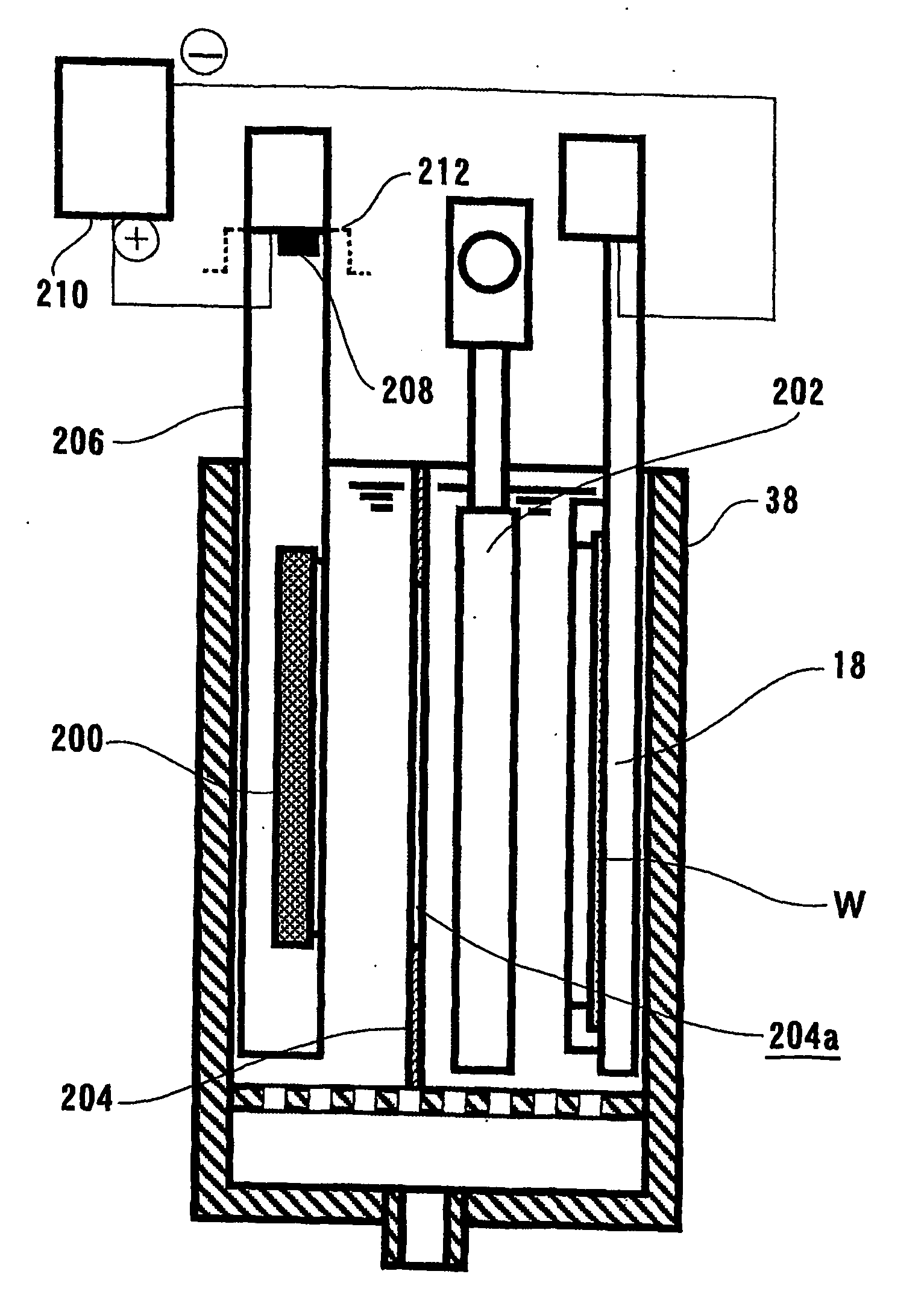
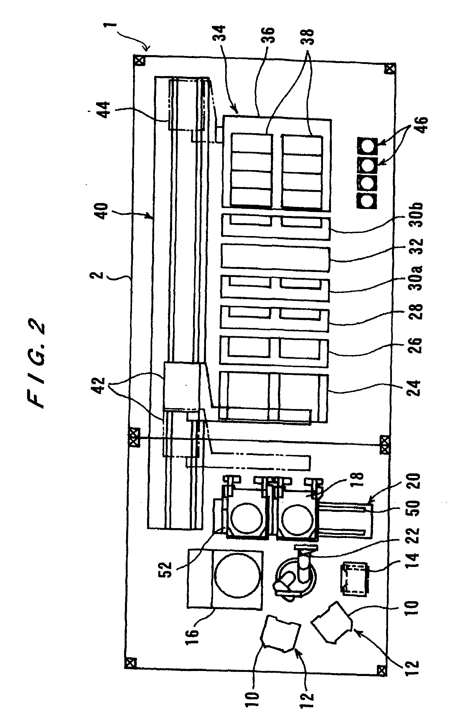
[0068]FIG. 2 is a schematic plan view showing a plating section 1 in a plating apparatus according to the present invention. As shown in FIG. 2, the plating section 1 has a rectangular frame 2, two cassette tables 12 each for placing thereon a cassette 10 which houses substrates such as semiconductor wafers, an aligner 14 for aligning an orientation flat or a notch of a substrate in a predetermined direction, and a cleaning and drying device 16 for cleaning a plated substrate and rotating the substrate at a high speed to dry the substrate. The cassette tables 12, the aligner 14, and the cleaning and drying device 16 are disposed along the same circle in the frame 2. The plating section 1 includes a substrate loading / unloading unit 20 disposed along a tangent line to the circle for loading a substrate onto and unloading a substrate from a substrate holder 18. The plating section 1 also has a substrate transfer device (transfer robot) 22 disposed at the center of the circle for transf...

second embodiment

[0148]FIG. 8 is a schematic plan view showing a plating apparatus according to the present invention. As shown in FIG. 8, the plating apparatus has a loading / unloading section 402 for loading and unloading cassettes 400 which house substrates such as semiconductor wafers therein, a tool stocker 404 for storing a plurality of types of tools (substrate holders) which correspond to the sizes of substrates to be plated, a transfer device 406 for transferring a substrate together with a tool holding the substrate, and a plating section 408.

[0149] The loading / unloading section 402 has sensors 410 provided at cassette holding portions on which cassettes 400 are mounted. The sensors 410 detect the sizes of the substrates received in the cassettes 400 on the cassette holding portions. Further, the loading / unloading section 402 has a substrate loading / unloading unit 412 disposed near the tool stocker 404 for loading a substrate onto and unloading a substrate from a tool. The substrate is tran...

third embodiment

[0158]FIG. 9 is a schematic plan view showing a plating apparatus according to the present invention. As shown in FIG. 9, the plating apparatus has one or more cassette tables 610 each for loading and unloading a substrate cassette housing substrates such as semiconductor wafers, two cleaning units 612, two pre-treatment units 614, two plating units 616, two resist stripping units 618, two etching units 620, and two reflowing units 622. In the illustrated example, the plating apparatus has three cassette tables 610. The cleaning units 612, the pre-treatment units 614, the plating units 616, the resist stripping units 618, the etching units 620, and the reflowing units 622 are independent of each other. As shown in FIG. 9, these units are incorporated integrally with each other so as to form two lines each including different types of units.

[0159] The plating apparatus also has a first transfer robot 624 disposed between the cassette tables 610 and the cleaning units 612 for transfer...


PUM

PropertyMeasurementUnit
heightaaaaaaaaaa
diameteraaaaaaaaaa
temperatureaaaaaaaaaa

Abstract

A plating apparatus has an ashing unit (300) configured to perform an ashing process on a resist (502) applied on a surface of a seed layer (500) formed on a substrate (W), and a pre-wetting section (26) configured to provide hydrophilicity to a surface of the substrate after the ashing process. The plating apparatus includes a pre-soaking section (28) configured to bring the surface of the substrate into contact with a treatment solution to clean or activate a surface of the seed layer formed on the substrate. The plating apparatus also includes a plating unit (34) configured to bring the surface of the substrate into a plating solution in a plating tank while the resist is used as a mask so as to form a plated film (504) on the surface of the seed layer formed on the substrate.

Description

TECHNICAL FIELD [0001] The present invention relates to a plating apparatus and a plating method for plating a surface of a substrate, and more particularly to a plating apparatus and a plating method for forming a bump (protruding electrode), which provides electrical connection with an electrode of a package or a semiconductor chip, on a surface of a semiconductor wafer while a resist is used as a mask. BACKGROUND ART [0002] In tape automated bonding (TAB) or flip chip, for example, it has widely been practiced to form protruding connecting electrodes (bumps) of gold, copper, solder, or nickel, or a multi-layer laminate of these metals at predetermined portions (electrodes) on a surface of a semiconductor chip having interconnects formed therein, and to electrically connect the interconnects via bumps with electrodes of a package or with TAB electrodes. In order to form bumps, there have been used various methods including electroplating, vapor deposition, printing, and ball bumpi...

Claims


Application Information

Patent Timeline
Patent Type & Authority Applications(United States)
IPC IPC(8): B05D1/32B05D3/00B05D1/18B05C11/00B05C3/00B05D5/00C25D5/02C25D7/12H01L21/00H01L21/288H01L21/60
CPCC25D5/022H01L21/2885H01L21/67173H01L21/6723H01L24/11H01L2224/1147H01L2224/13099H01L2924/01029H01L2924/01046H01L2924/01047H01L2924/01074H01L2924/01078H01L2924/01079H01L2924/01082H01L2924/01322H01L2924/01006H01L2924/01033H01L2924/014C25D7/123C25D17/001H01L2224/05573H01L2224/05568H01L2224/05647H01L2924/00014
Inventor SEKIMOTO, MASAHIKOENDO, YASUHIKOSTRAUSSER, STEPHENTAKEMURA, TAKASHISAITO, NOBUTOSHIKURIYAMA, FUMIOYOSHIOKA, JUNICHIROHORIE, KUNIAKIMINAMI, YOSHIO
Owner EBARA CORP
Why Eureka
Try Eureka