Method for forming shallow trench isolation in semiconductor device

Inactive Publication Date: 2006-07-06
DONGBU ELECTRONICS CO LTD
View PDF8 Cites 15 Cited by
  • Summary
  • Abstract
  • Description
  • Claims
  • Application Information

AI Technical Summary

Benefits of technology

[0012] It is, therefore, an object of the present invention to provide a method for forming shallow trench isolation with n

Problems solved by technology

However, according to the increase of the integration density, a LOCOS field oxide has become disadvantageous to the formation of integrated circuits, because it generally includes a “bird's beak,” which may invade an active device region.
Excessive decreasing of the slope of trench 20 may result in defects (e.g., dislocations) in

Method used


Image

  • Method for forming shallow trench isolation in semiconductor device
  • Method for forming shallow trench isolation in semiconductor device
  • Method for forming shallow trench isolation in semiconductor device

Examples


Example

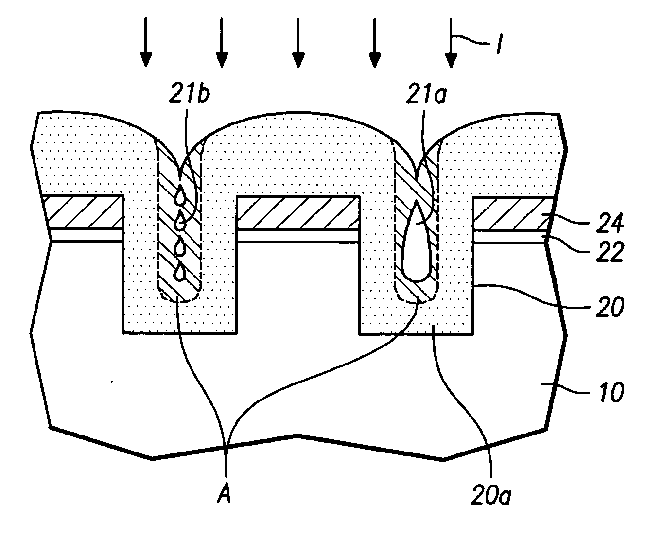
[0019]FIG. 2A shows a cross-sectional view of a shallow trench isolation structure, wherein trenches 20 are formed in a substrate 10, and then are filled with a first filling oxide 20a. Namely, a pad oxide 22 and a pad nitride 24 are formed on the substrate 10 in successive order. Then, a moat pattern (i.e., a photoresist pattern) is formed by a photolithography process. The moat pattern defines openings over regions of the substrate 10, the pad oxide 22, and the pad nitride 24 in which a trench structure 20 may be formed. Subsequently, after the pad nitride 24 and the pad oxide 22 are etched, the exposed portion of the substrate 10 is also etched in a predetermined depth so that trenches 20 are formed. Further, trenches 20 are filled with the first filling oxide 20a. Before the first filling process, a liner oxide is preferably formed on the sidewall of trench 20 by an oxidation process. After the liner oxidation, the first filling oxide 20a is formed in trenches 20 and over the en...


PUM


Abstract

A method for forming shallow trench isolation in a semiconductor device. The method includes forming a trench in a predetermined depth on a semiconductor substrate, filling the trench with a first filing oxide, injecting an impurity into a portion of the first filling oxide inside the trench, removing the portion of the first filling oxide by wet etching, and filling the trench with a second filling oxide.

Description

[0001] This application claims the benefit of Korean Application No. 10-2004-0117500, filed with the Korean Intellectual Property Office on Dec. 30, 2004, which is incorporated by reference herein in its entirety. BACKGROUND OF THE INVENTION [0002] 1. Field of the Invention [0003] The present invention relates generally to a semiconductor device manufacturing technology, and particularly to a method for forming shallow trench isolation in a semiconductor device. [0004] 2. Description of the Related Art [0005] Manufacturing processes for making a highly integrated semiconductor device requires forming a variety of components, such as a transistor, capacitor, metal wiring, etc., in very restricted regions, and forming highly insulated regions to prevent parasitic current leakage between the components. [0006] Conventionally, a local oxidation of silicon (LOCOS) field oxide, formed by oxidizing a silicon substrate, has been widely used for electrically isolating the components of the s...

Claims


Application Information

Patent Timeline
IPC IPC(8): H01L21/76
CPCH01L21/76224H01L21/76H01L21/762
Inventor KIM, WAN SHICK
Owner DONGBU ELECTRONICS CO LTD
Why Eureka
Try Eureka