Wafer level test head

a test head and wafer technology, applied in the direction of electrical testing, measurement devices, instruments, etc., can solve the problems of limiting the speed of wafer sort testing, % of the total chips are typically defective, and the use of probe cards is extremely complex, so as to relieve tensile/compressive stresses and reduce the effect of shear stress

Inactive Publication Date: 2006-07-06
SALMON PETER C
View PDF4 Cites 20 Cited by
  • Summary
  • Abstract
  • Description
  • Claims
  • Application Information

AI Technical Summary

Benefits of technology

[0005] The current invention is a test head that can be used for parallel testing and/or burn-in of a wafer full of high-powered logic chips such as microprocessors. A test pedestal includes connections to a power source and a test support computer. Test circuits are mounted on a test execution wafer supported on the test pedestal, connected to the power source and the test support computer. The preferred method for mounting chips on the test execution wafer employs an advanced flip chip connector. Each connector includes a copper spring element inserted into a well filled with solder; the spring elements attach to input/output (I/O) pads of attac

Problems solved by technology

The probes typically have inductance that limits the speed of wafer sort testing.
Around 10-20% of the total chips are typically defective at wafer sort.
For logic circuits like microprocessors havi

Method used


Image

  • Wafer level test head
  • Wafer level test head
  • Wafer level test head

Examples


Embodiment Construction

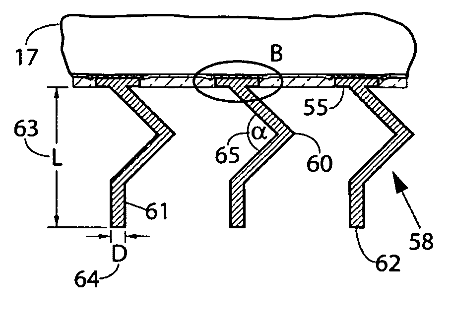
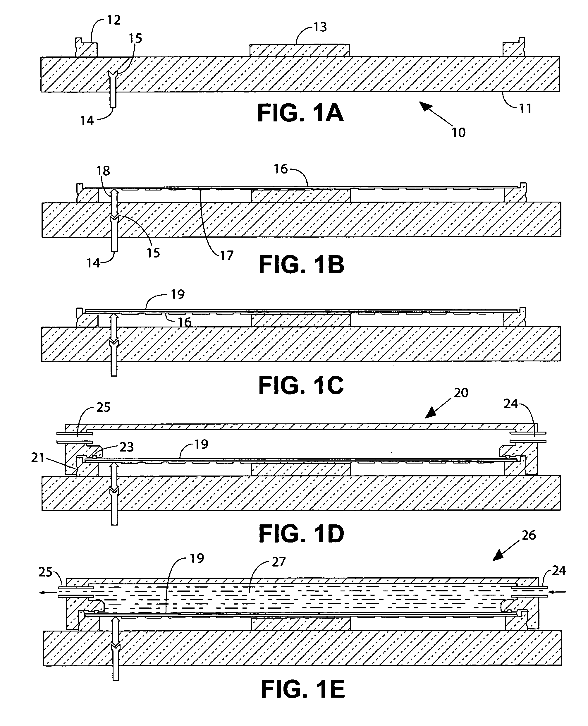
[0022]FIG. 1A-1E details a sequence of steps to configure and operate a wafer level test head of the current invention. The reference case will be assumed: 177 microprocessor die on a bumped 300 mm wafer, with each die dissipating 120 watts of heat. The total heat generated during testing is over 20,000 watts.

[0023]FIG. 1A shows a test pedestal 10 including a base plate 11, a support ring 12, a center support 13, and electrical input / outputs 14 terminating in a connector 15. Electrical input / outputs 14 include a power source such as 42 volts DC, plus an interface to a test support computer, as will be further described.

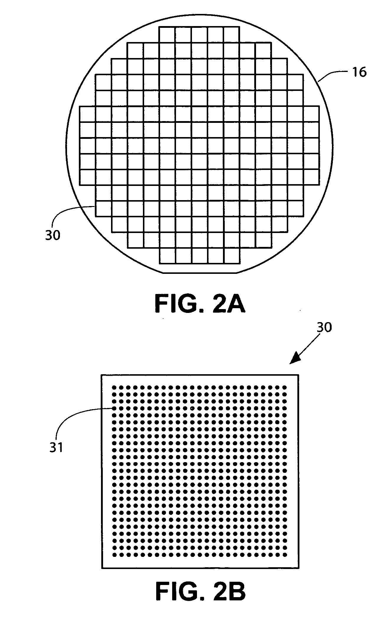
[0024] In FIG. 1B test execution wafer 16 is positioned on pedestal 10 using support ring 12 and center support 13. Test execution wafer 16 has an array of integrated circuit (IC) chips like 17 mounted on its bottom side. These chips will perform all test execution and power distribution functions, as will be further described. They are attached using improved flip ...


PUM


Abstract

A test head is described for simultaneous test and/or simultaneous burn-in of all of the chips on a semiconductor wafer, including high powered microprocessor chips. A test execution wafer is attached to a test pedestal with connections for power plus an interface to a test support computer. Mounted on the test execution wafer are all of the IC chips required to implement test circuits, power distribution, local memory, temperature sensing, and communication interfaces. Advanced flip chip connectors are preferably employed for assembling the test execution wafer; they enable rework of any chips that prove defective. Embedded in the test execution wafer are general purpose interconnection circuits plus through-wafer connectors. A test socket employing wells filled with liquid metal is provided on the back side of the test execution wafer. The wafer under test is bumped at the I/O pads, and the bumps are inserted into the wells filled with liquid metal. By circulating water or other cooling fluid against the back side of the wafer under test, a cooling rate of 20,000 watts or more can be applied.

Description

[0001] This invention relates to apparatus and methods for testing electronic components, and more particularly to apparatus and methods for simultaneous testing of all the die on a wafer, including high powered microprocessors. BACKGROUND OF THE INVENTION [0002] The current practice for testing integrated circuit (IC) chips and the systems using them includes wafer sort at the wafer level, class test at the packaged component level, board test at the board level, and system test at the system level. At wafer sort, typically the wafer is tested one chip at a time, using a probe card that steps in sequence across the wafer. The probes typically have inductance that limits the speed of wafer sort testing. Around 10-20% of the total chips are typically defective at wafer sort. The remaining good chips are assembled into discrete packages and class tested, typically at full clock speed. If burn-in is required it is usually performed using packaged parts; they are plugged into sockets on...

Claims


Application Information

Patent Timeline
IPC IPC(8): G01R31/02
CPCG01R1/07357G01R31/2886
Inventor SALMON, PETER C.
Owner SALMON PETER C
Why Eureka
Try Eureka