Current-reuse-type frequency multiplier

a frequency multiplier and current-reuse technology, applied in the field of frequency multipliers, can solve the problems of difficult to obtain sufficient output oscillation at a power supply voltage of 1.8 v, easy to affect the operation of the first n-channel mos transistor, etc., and achieve the effect of reducing the inductance effect of ground wiring

Inactive Publication Date: 2006-07-06
MITSUBISHI ELECTRIC CORP
View PDF3 Cites 19 Cited by
  • Summary
  • Abstract
  • Description
  • Claims
  • Application Information

AI Technical Summary

Benefits of technology

[0008] It is an object of this invention to provide a current-reuse-type frequency multiplier capable of reducing the effect of inductance of ground wiring.
[0010] The effect of inductance of ground wiring connected to the first and second transistors can be reduced.

Problems solved by technology

However, in a Gilbert-Cell frequency multiplier that has conventionally been in widespread use, where a plurality of transistors are stacked vertically in three tiers between a power supply line and a ground line, sufficient output oscillation would be difficult to obtain at a power supply voltage of 1.8 V.
In such ways, there has been a problem with this conventional frequency doubler in that the operation of the first N-channel MOS transistor is easily affected by the inductance of the ground wire.

Method used


Image

  • Current-reuse-type frequency multiplier
  • Current-reuse-type frequency multiplier
  • Current-reuse-type frequency multiplier

Examples


first preferred embodiment

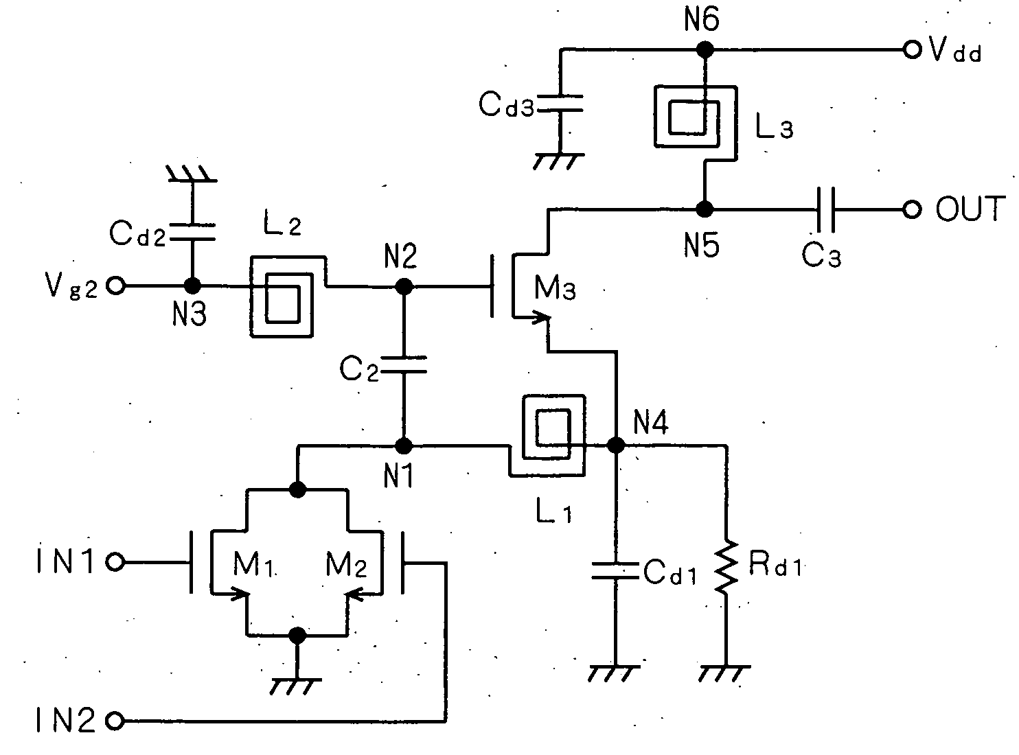
[0025]FIG. 1 is a circuit diagram illustrating the structure of a current-reuse-type frequency doubler according to a first preferred embodiment of this invention. As shown, this current-reuse-type frequency doubler includes differential input terminals IN1 and IN2, an output terminal OUT, N-channel MOS transistors M1, M2 and M3, capacitors Cd1, Cd2, Cd3, C2 and C3, inductors L1, L2 and L3, and a resistance element Rd1. The inductors L1, L2 and L3 are formed of spiral inductors, for example.

[0026] Provided in the front stage of the current-reuse-type frequency doubler is a VCO (not shown) of differential operation having two differential output terminals. The differential input terminal IN1 is connected to one of the differential output terminals of the VCO, and the differential input terminal IN2 to the other differential output terminal of the VCO. RF signals in a complementary relationship with each other that are output from the VCO are input to the differential input terminals...

second preferred embodiment

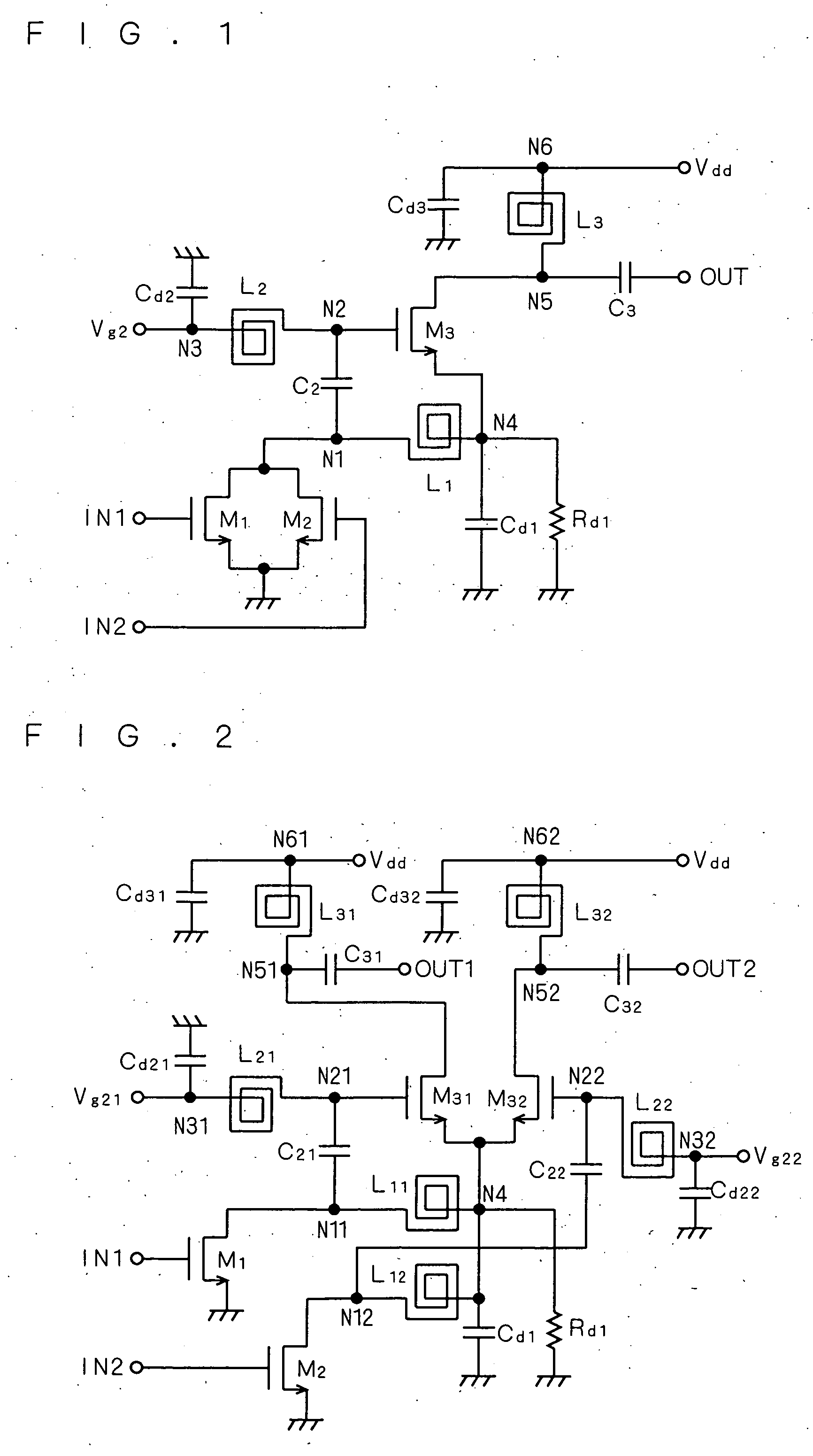
[0041] A current-reuse-type frequency doubler having an input formed in a differential manner was described in the first preferred embodiment. Described in a second preferred embodiment is a current-reuse-type frequency doubler having both an input and an output formed in a differential manner.

[0042]FIG. 2 is a circuit diagram illustrating the structure of a current-reuse-type frequency doubler according to the second preferred embodiment of this invention. As shown, this current-reuse-type frequency doubler includes differential input terminals IN1 and IN2, differential output terminals OUT1 and OUT2, N-channel MOS transistors M1, M2, M31 and M32, capacitors Cd1, Cd21, Cd22, Cd31, Cd32; C21, C22, C31 and C32, inductors L11, L12, L21, L22, L3, and L32, and a resistance element Rd1. The inductors L11, L12, L21, L22, L31 and L32 are made of spiral inductors, for example.

[0043] Provided in the front stage of the current-reuse-type frequency doubler is a VCO (not shown) of differentia...

third preferred embodiment

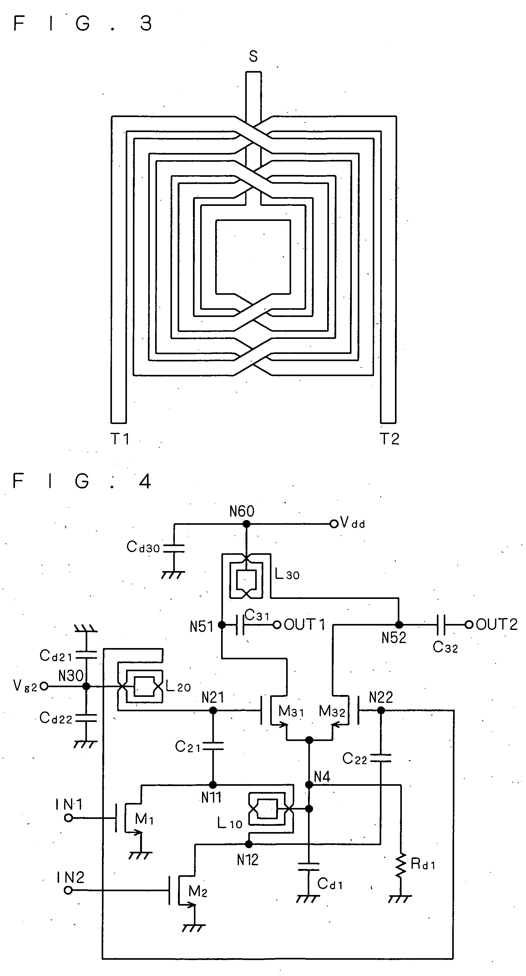
[0057]FIG. 3 is a top view schematically illustrating the structure of a differential inductor. The differential inductor is a combination of a first spiral inductor having a terminal S as one end and a terminal T1 as a first other end, and a second spiral inductor having the terminal S as one end and a terminal T2 as a second other end, both of which are formed in the same region by using a plurality of wiring layers of multilevel wiring structure.

[0058] In a third preferred embodiment, the differential inductor is used to form the current-reuse-type frequency doubler according to the second preferred embodiment.

[0059]FIG. 4 is a circuit diagram illustrating the structure of a current-reuse-type frequency doubler according to the third preferred embodiment of this invention. As shown, this current-reuse-type frequency doubler includes differential input terminals IN1 and IN2, differential output terminals OUT1 and OUT2, N-channel MOS transistors M1, M2, M31 and M32, capacitors Cd...


PUM


Abstract

A first differential input terminal is connected to one differential output terminal of a VCO, and a second differential input terminal is connected to the other differential output terminal of the VCO. RF signals in a complementary relationship with each other that are output from the VCO are input to the first and second differential input terminals as input signals. The gate of a first N-channel MOS transistor is connected to the first differential input terminal, and the gate of a second N-channel MOS transistors is connected to the second differential input terminal. The sources of the first and second N-channel MOS transistors are connected to a ground potential. The drains of the first and second N-channel MOS transistors are commonly connected to a node.

Description

BACKGROUND OF THE INVENTION [0001] 1. Field of the Invention [0002] This invention relates to frequency multipliers, and more particularly to current-reuse-type frequency multipliers. [0003] 2. Description of the Background Art [0004] A frequency multiplier has the function of converting an RF (Radio Frequency) signal output from a voltage control oscillator (hereafter referred to as a “VCO”) into a harmonic having a frequency which is an integral multiple of the fundamental frequency in a wireless system and the like. Recent technological progress toward finer CMOS has allowed the VCO and frequency multiplier to be integrated on an RF transceiver chip, resulting in numerous wireless LSIs being announced and put on the market. As CMOSs become finer, however, a gate breakdown voltage decreases, which requires an operating-voltage to decrease in each circuit block. For example, in a CMOS having a gate length of 0.18 μm, where an operation from a 1.8 V source is usually required, each ...

Claims


Application Information

Patent Timeline
Patent Type & Authority Applications(United States)
IPC IPC(8): H03B19/00
CPCH03B19/14
Inventor YAMAMOTO, KAZUYAKITABAYASHI, FUMIMASA
Owner MITSUBISHI ELECTRIC CORP
Why Eureka
Try Eureka