Method of laser processing a wafer

a laser processing and wafer technology, applied in the field of laser processing a wafer, can solve the problems of other problems in respect of productivity, damage devices, and problems in manufacturing tools, and achieve the effects of preventing the flaking of a layer

Inactive Publication Date: 2006-07-13
DISCO CORP
View PDF5 Cites 15 Cited by
  • Summary
  • Abstract
  • Description
  • Claims
  • Application Information

AI Technical Summary

Benefits of technology

[0010] a first groove forming step for applying a first laser beam having absorptivity for the wafer along the streets of the wafer at predetermined intervals to form two grooves for preventing the flaking of a layer, which divide the laminate layer; and
[0011] a second groove forming step for applying a second laser beam having absorptivity for the wafer to the center between the two grooves for preventing the flaking of a layer, which have been formed along the streets of the wafer by the first groove forming step, along the streets of the wafer to form a dividing groove having a predetermined depth in the laminate layer and the substrate.
[0012] In the wafer laser processing method according to the present invention, since the second groove forming step for forming a dividing groove having a predetermined depth in the laminate layer and the substrate at the center between two grooves for preventing the flaking of a layer is carried out after the two grooves for preventing the flaking of a layer, which divide the laminate layer, are formed along the streets of the wafer by the first groove forming step, the laminate layer in the streets is divided by the two grooves for preventing the flaking of a layer when the second groove forming step is carried out. Therefore, even if the laminate layer flakes off by the application of the second pulse laser beam, the flaking does not affect the outer sides of the two grooves, that is, the sides of the devices. Consequently, the pulse energy of the second pulse laser can be increased, and the dividing groove can be formed to a desired depth that facilitates division of the wafer.

Problems solved by technology

Since the optical device wafer is made of a material having extremely high hardness, it cannot be cut with the cutting blade at a rate of 10 mm / sec or less, thereby making a problem in respect of productivity.
Further, a cutting blade having a thickness of about 250 μm must be used to cut the optical device wafer, chippings are large in size and hence, the width of each street must be made 300 μm or more, thereby causing other problems in respect of productivity.
When a high-output laser beam is applied to the wafer, however, the laminate layer may flake off about 100 to 200 μm on one side by an impact made by the application of the laser beam, thereby damaging devices.

Method used


Image

  • Method of laser processing a wafer
  • Method of laser processing a wafer
  • Method of laser processing a wafer

Examples


Embodiment Construction

[0023] The wafer laser processing method of the present invention will be described in more detail hereinunder with reference to the accompanying drawings.

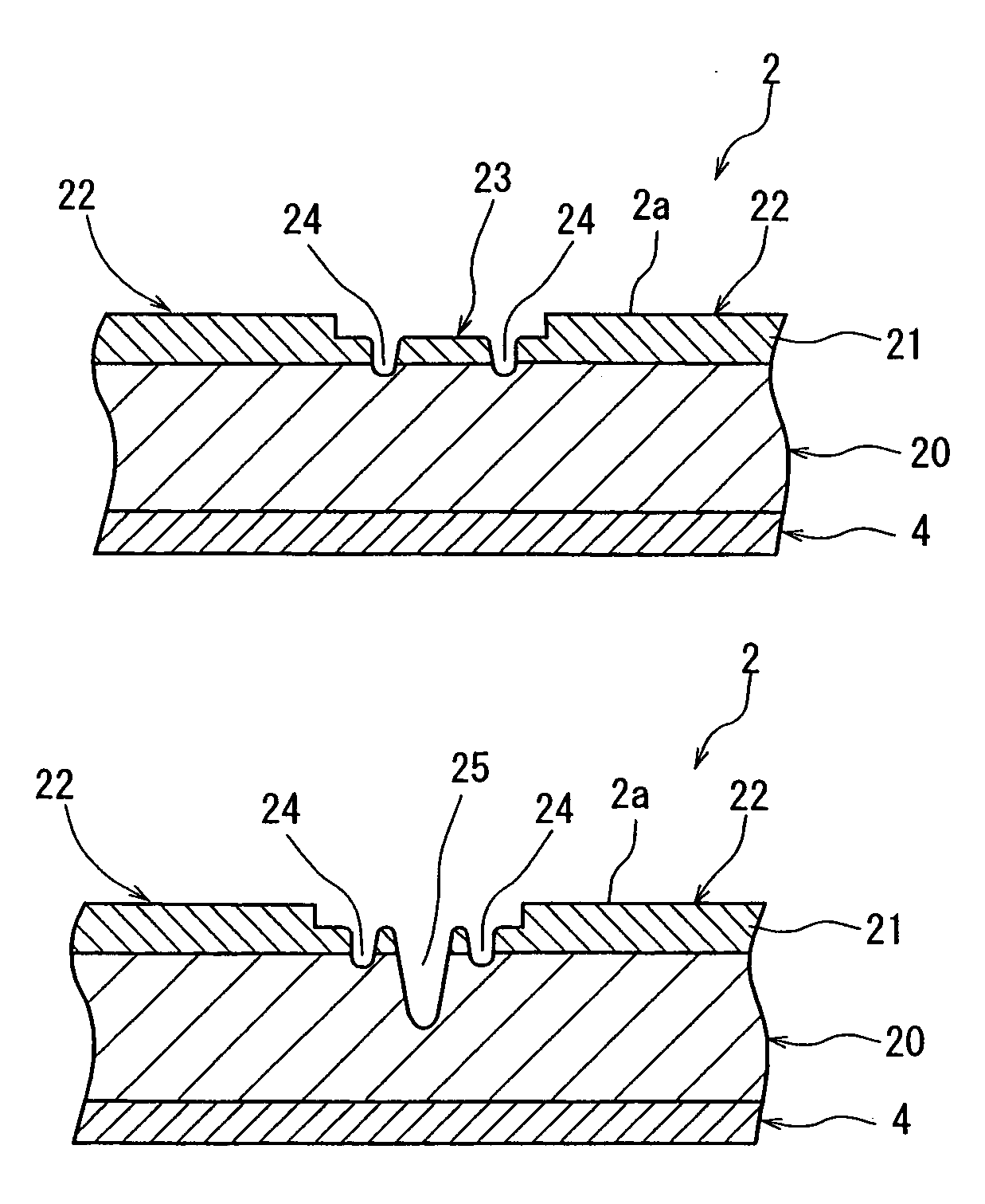
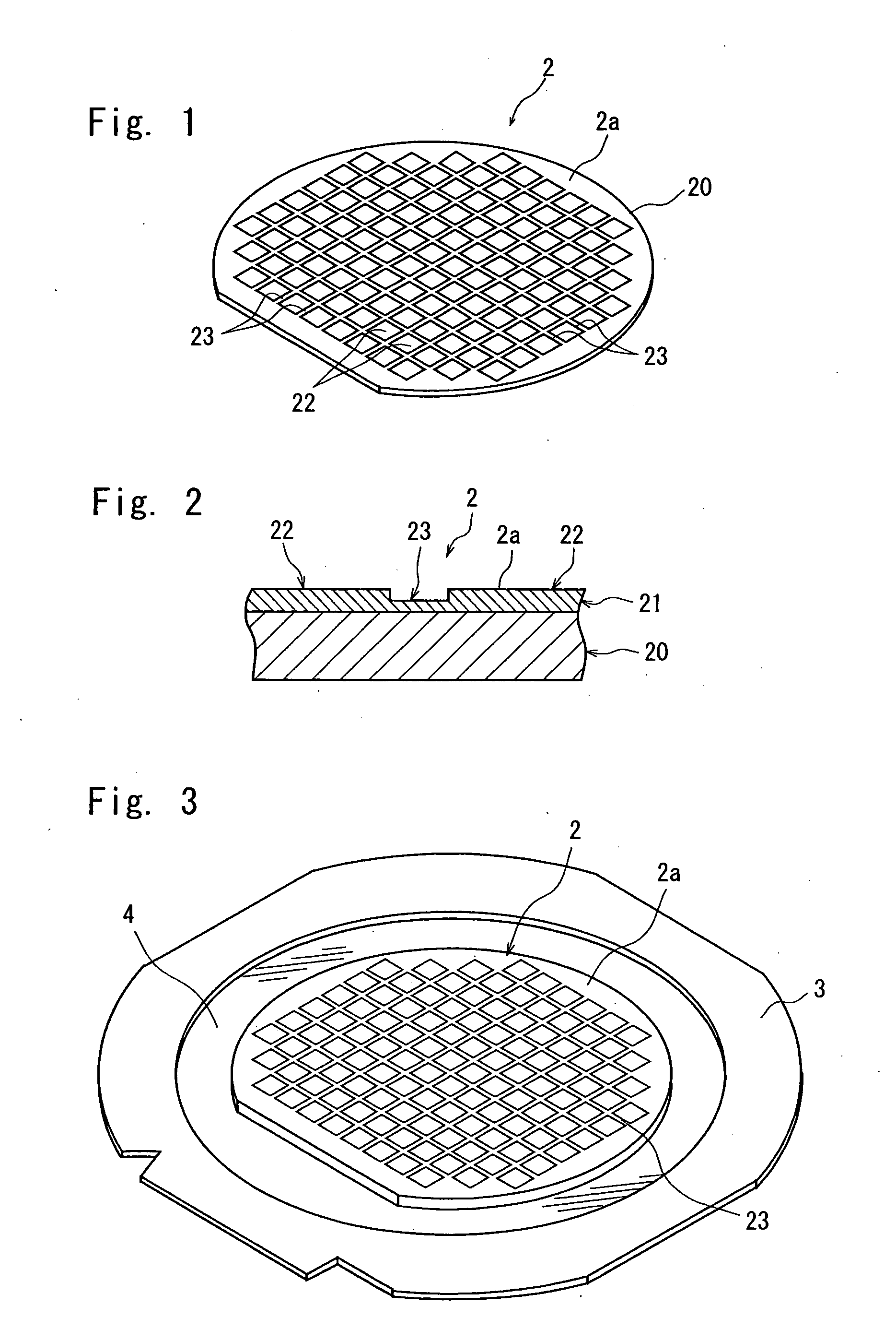
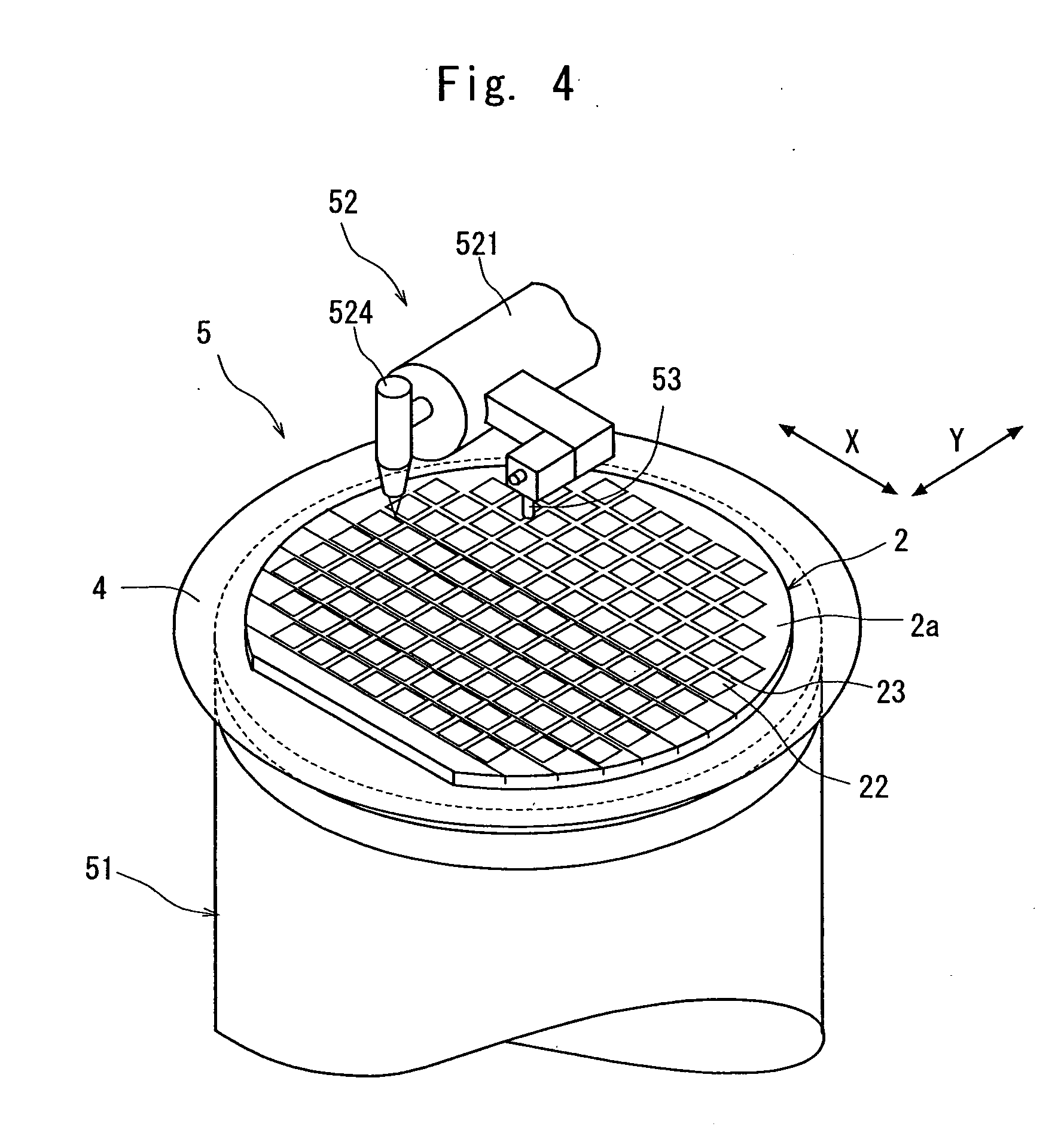
[0024]FIG. 1 is a perspective view of an optical device wafer to be divided into individual chips by the wafer laser processing method of the present invention, and FIG. 2 is an enlarged sectional view of the principal portion of the optical device wafer shown in FIG. 1. The optical device wafer 2 shown in FIG. 1 and FIG. 2 has a plurality of devices 22 which are composed of a laminate layer 21 comprising a layer having a wavelength discriminating filter function to transmit only light having a specific wavelength or a specific wavelength range and reflect light having other wavelengths and formed in a matrix on the front surface of a substrate 20 made of quartz, borosilicate glass or the like. The devices 22 are sectioned by streets 23 formed in a lattice pattern. In the illustrated embodiment, laminates forming the laminate lay...


PUM

PropertyMeasurementUnit
diameteraaaaaaaaaa
thicknessaaaaaaaaaa
thicknessaaaaaaaaaa

Abstract

A method of laser processing a wafer having a plurality of devices that are composed of a laminate layer laminated on the front surface of a substrate, along a plurality of streets for sectioning the devices, comprising a first groove forming step for applying a first laser beam having absorptivity for the wafer along the streets of the wafer at predetermined intervals to form two grooves for preventing the flaking of a layer, which divide the laminate layer; and a second groove forming step for applying a second laser beam having absorptivity for the wafer to the center between the two grooves for preventing the flaking of a layer, which have been formed along the streets of the wafer by the first groove forming step, along the streets of the wafer to form a dividing groove having a predetermined depth in the laminate layer and the substrate.

Description

FIELD OF THE INVENTION [0001] The present invention relates to a method of laser processing a wafer having a plurality of devices, which are composed of a laminate layer laminated on the front surface of a substrate along streets formed on the front surface of the wafer. DESCRIPTION OF THE PRIOR ART [0002] As is known to people of ordinary skill in the art, an optical device wafer having a plurality of optical devices which are composed of a laminate layer of silicon oxide (SiO2) and the like that discriminates a specific wavelength, and formed in a matrix on the front surface of a substrate made of quartz, glass or the like is manufactured in the production process of an optical device. The above optical devices are sectioned by dividing lines called “streets” in the thus-formed optical device wafer, and individual optical devices are manufactured by dividing this optical device wafer along the streets. [0003] Dividing along the streets of the above optical device wafer is generall...

Claims


Application Information

Patent Timeline
Patent Type & Authority Applications(United States)
IPC IPC(8): H01L21/78H01L21/301H01L21/46
CPCB23K26/367B23K26/4075H01L21/3043H01L21/67092H01L21/78B23K26/364B23K26/40B23K2103/50
Inventor KOBAYASHI, SATOSHI
Owner DISCO CORP
Why Eureka
Try Eureka