Fabrication of MOS-gated strained-Si and SiGe buried channel field effect transistors

Inactive Publication Date: 2006-07-20
EPISPEED
View PDF0 Cites 22 Cited by
  • Summary
  • Abstract
  • Description
  • Claims
  • Application Information

AI Technical Summary

Benefits of technology

[0022] The present invention provides a method for the fast growth of heterostructures comprising a strain relaxed buffer layer on Si substrates (virtual substrate, VS) with an active layer stack on top. The structures are especially suitable for the fabricatio

Problems solved by technology

Unfortunately, these are usually accompanied by so-called threading dislocations (TDs).
Although consumer applications of such two dimensional devices, such as MODFETS have been somewhat limited, they are used in satellite television receivers where the frequency range of GaAs and the low-noise behaviour of modulation-doped devices come into play.
They suffer, however, from interface scattering at the oxide/silicon interface.
Buried channel devices are on the other hand characterized by reduced scattering at the smoother epitaxial interfaces at the expense of poorer gate control because of the larger gate to channel distance.
Device performance was limited, however, due to transport through the low-m

Method used


Image

  • Fabrication of MOS-gated strained-Si and SiGe buried channel field effect transistors
  • Fabrication of MOS-gated strained-Si and SiGe buried channel field effect transistors
  • Fabrication of MOS-gated strained-Si and SiGe buried channel field effect transistors

Examples


Embodiment Construction

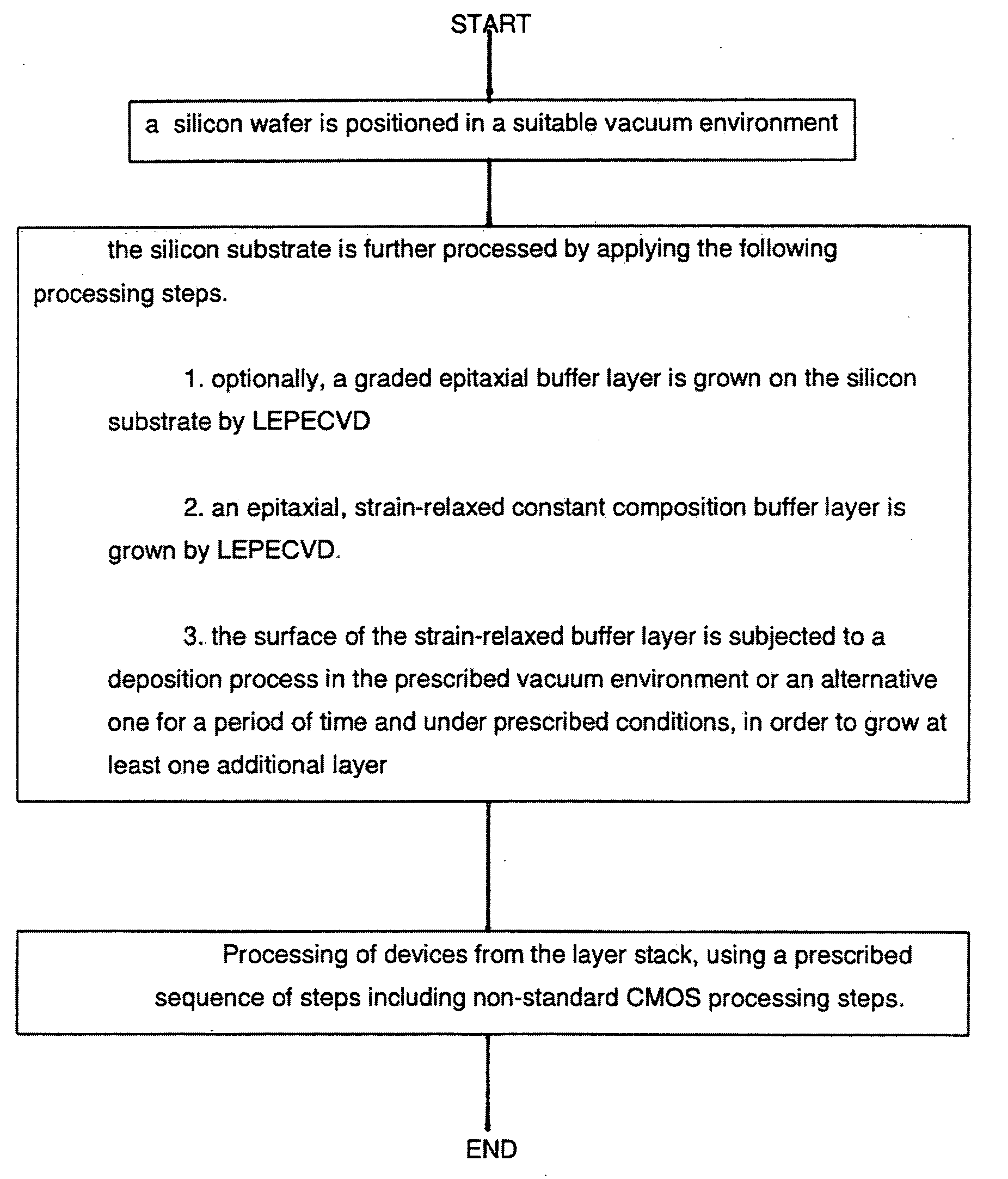
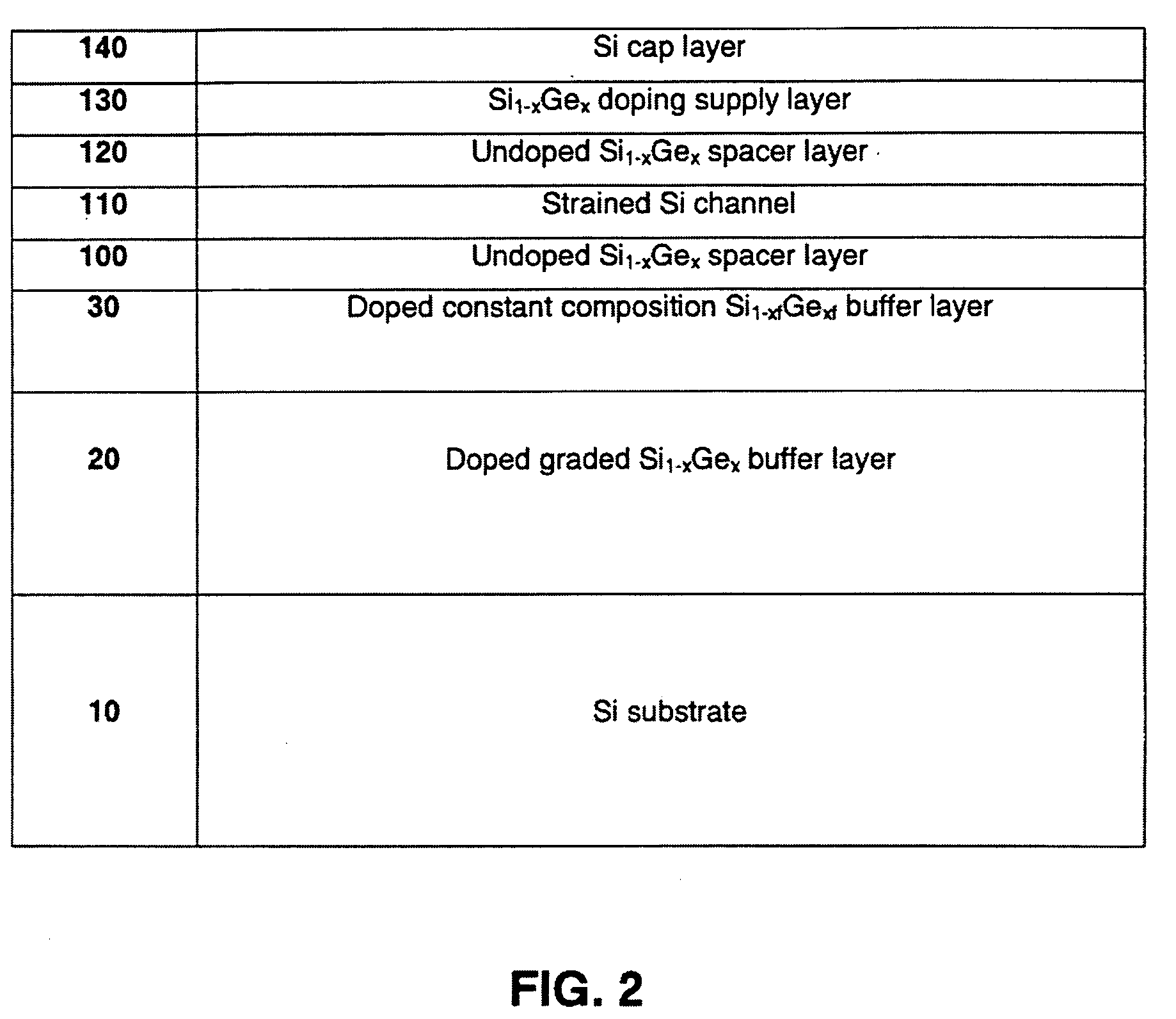
[0036] Referring now to FIG. 1, a method is provided for fabricating semiconductor heterostructures. The method includes the following three steps. In a first step 4, a silicon wafer is positioned in a suitable environment, such as a vacuum chamber equipped with a substrate heater and components suitable for epitaxial layer deposition. In a second step 6, the silicon substrate is further processed by applying several processing steps. In a first optional processing step 6a, an epitaxial graded buffer layer is grown on a the silicon substrate by low-energy plasma-enhanced chemical vapor deposition (LEPECVD). In a second processing step 6b, an epitaxial strain-relaxed constant composition buffer layer is grown by LEPECVD. In a third processing step 6c the surface of the strain-relaxed buffer layer is subjected to a deposition process for a period of time and under prescribed conditions, in order to grow at least one additional layer. In a third step 8, device processing is carried out...


PUM


Abstract

A method of fabricating semiconductor heterostructures including the steps of: (a) positioning a silicon wafer in a suitable environment and (b) processing the silicon substrate by applying several processing steps. A first optional processing step includes growing a graded buffer layer on a silicon substrate by low-energy plasma-enhanced chemical vapor deposition (LEPECVD). A second processing step includes growing a constant composition buffer layer by LEPECVD. A third processing step includes subjecting the surface of the strain-relaxed buffer layer to a deposition process for a period of time and under prescribed conditions, in order to grow at least one additional layer. Subsequently, devices may be processed from the grown layer stack by using a prescribed sequence of steps including non-standard CMOS processes.

Description

BACKGROUND OF THE INVENTION [0001] The invention relates to the field of strained semiconductor structures on top of a strain-relaxed buffer layer, which can be applied in particular to the fabrication of integrated circuits comprising buried-channel and surface-channel strained-Si field effect transistors with a metal-oxide gate. [0002] The beneficial role of tensile strain for enhancing the electronic properties of Si was recognized in the mid eighties by Abstreiter et al. (see Abstreiter et al., Phys. Rev. Lett. 54, 2441 (1985)), the content of which is incorporated herein by reference hereto. [0003] Nearly 20 years of intense research on strained-Si have followed this initial discovery (see for example Schäffler, Semicond. Sci. Technol. 12, 1515 (1997), the content of which is incorporated herein by reference hereto). The most common way to impose tensile strain is by epitaxial growth. A relaxed buffer layer or virtual substrate (VS) with lattice parameter larger than that of Si...

Claims


Application Information

Patent Timeline
IPC IPC(8): H01L31/109
CPCH01L21/02381H01L21/0245H01L21/02505H01L21/0251H01L21/02532H01L29/66431H01L29/7782
Inventor VON KAENEL, HANSFOBELETS, KRISTELHACKBARTH, THOMAS
Owner EPISPEED
Why Eureka
Try Eureka