Metal-insulator-metal capacitor and method of fabricating the same

a technology of metal-insulator and capacitor, which is applied in the direction of capacitors, semiconductor devices, electrical equipment, etc., can solve the problems of reducing the overall capacitance value, unsatisfactory voltage linearity of conventional mos or mis capacitors commonly employed in contemporary systems,

Inactive Publication Date: 2006-07-20
SAMSUNG ELECTRONICS CO LTD
View PDF2 Cites 25 Cited by
  • Summary
  • Abstract
  • Description
  • Claims
  • Application Information

AI Technical Summary

Benefits of technology

[0011] The present invention provides a metal-insulator-metal (MIM) capacitor capable of preventing the generation of a crack in a dielectric layer under an upper electrode pattern.

Problems solved by technology

Conventional MOS or MIS capacitors commonly employed in contemporary systems not only have unsatisfactory voltage linearity that arises from voltage-induced space charge regions but also numerous sources of parasitic capacitance.
However, since the PIP capacitors use conductive polysilicon for an upper electrode layer and a lower electrode layer, an oxidation reaction occurs in the interfaces between upper and lower electrodes and a dielectric layer, resulting in the formation of a natural oxide film and thus reduction of the overall capacitance value.

Method used


Image

  • Metal-insulator-metal capacitor and method of fabricating the same
  • Metal-insulator-metal capacitor and method of fabricating the same
  • Metal-insulator-metal capacitor and method of fabricating the same

Examples


first embodiment

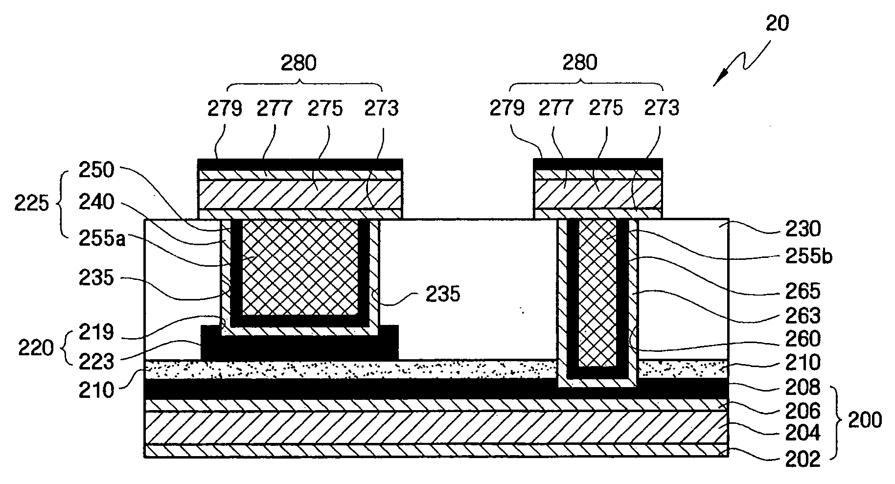
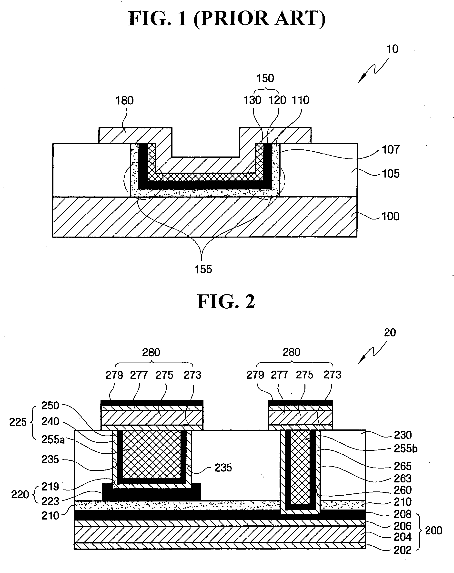
[0057]FIG. 2 is a cross sectional view of an MIM capacitor 20 according to the present invention.

[0058] Referring to FIG. 2, the MIM capacitor 20 includes a lower electrode pattern 200, a dielectric pattern 210, an upper electrode layer 220, and an interlayer insulating layer 230.

[0059] A four-layer structure of TiN / Ti / Al / Ti layers 208, 206, 204, 202 is used for the lower electrode pattern 200. The TiN layer 208 is formed for preventing diffusion. The Ti layer 206 is formed for adhesion. The Al layer 204 has excellent electrical conductivity and is used as a base of a lower electrode layer. The Ti layer 202 functions as a barrier for preventing diffusion between a lower substrate (not shown) and the Al layer 204.

[0060] The dielectric pattern 210 is formed on the lower electrode pattern 200 and may comprise, for example, SiN, Al2O3, Ta2O5, TiO, (Ba,Sr)TiO3, Pb(Zr,Ti)O3, or (Pb,La)(Zr,Ti)O3. In the present invention, SiN is used for the dielectric pattern 210.

[0061] The upper elect...

second embodiment

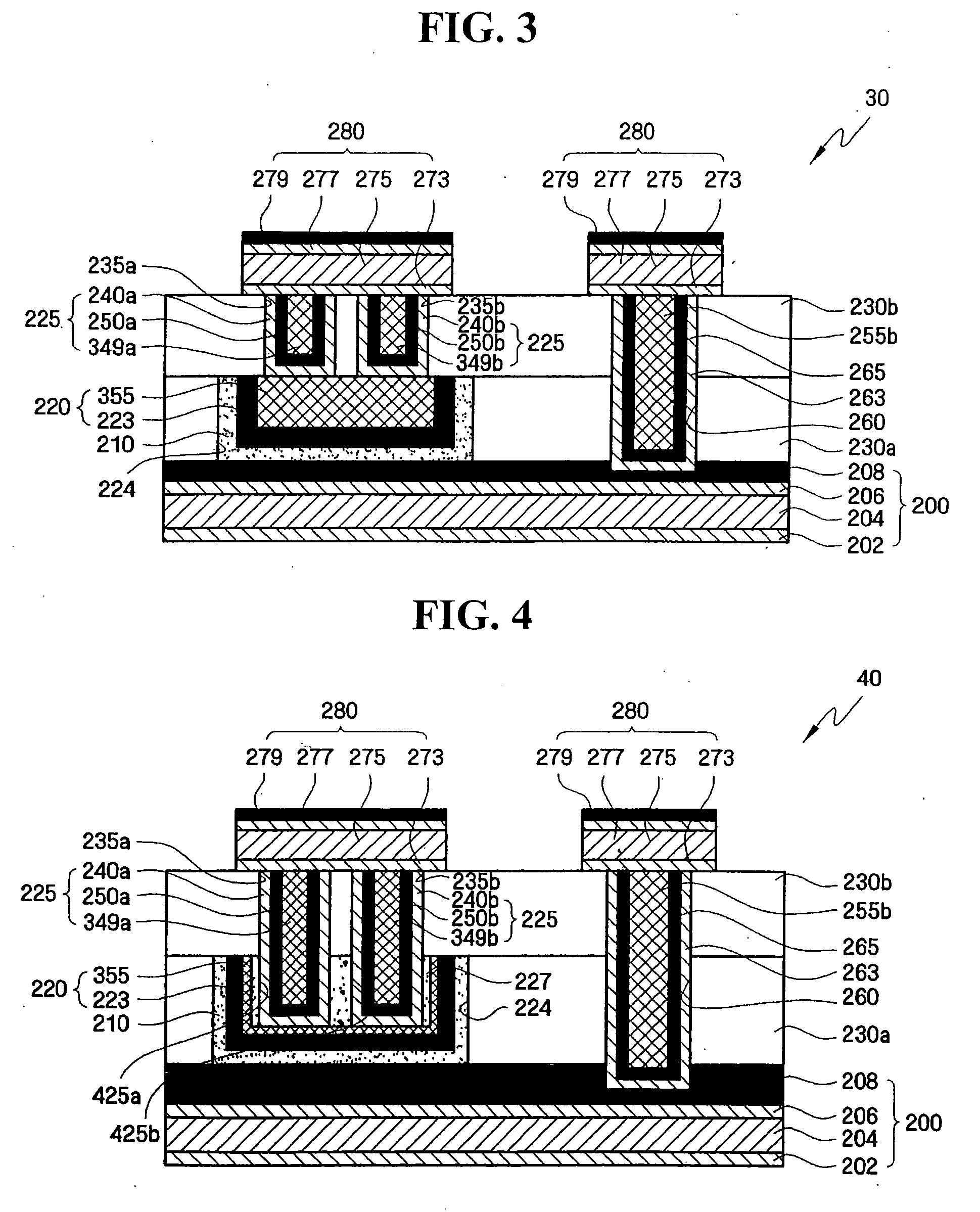
[0080]FIG. 3 is a cross sectional view of an MIM capacitor according to the present invention.

[0081] In FIGS. 2 and 3, like reference numerals refer to like elements.

[0082] An MIM capacitor 30 according to a second embodiment of the present invention includes a lower electrode pattern 200, a first interlayer insulating layer 230a, a dielectric layer 210, an upper electrode layer 220, a second interlayer insulating layer 230b, and an upper interconnect 280.

[0083] Hereinafter, only a difference between the MIM capacitor 20 according to the first embodiment of the present invention and the MIM capacitor 30 according to the second embodiment of the present invention and other points that are not explained in the above description will be described.

[0084] The first interlayer insulating layer 230a is formed on the lower electrode pattern 200 and its upper surface is planarized.

[0085] An opening pattern 224 that exposes the lower electrode pattern 200 is formed in the first interlayer...

third embodiment

[0093]FIG. 4 is a cross sectional view of an MIM capacitor according to the present invention.

[0094] In FIGS. 3 and 4, like reference numerals refer to like elements.

[0095] As shown in FIG. 4, in an MIM capacitor 40 according to a third embodiment of the present invention, the structures of an opening pattern 224 and a via 225 are different from those in the MIM capacitor 30 according to the second embodiment of the present invention.

[0096] In other words, the opening pattern 224 includes the conformally formed dielectric layer 210 and the upper electrode layer 220 that fills the opening pattern 224 in the MIM capacitor 30 according to the second embodiment of the present invention, but the dielectric layer 210 and the upper electrode layer 220 are conformally formed in the opening pattern 224 and a filling insulating layer 227 fills the opening pattern 224 in the MIM capacitor 40 according to the third embodiment of the present invention.

[0097] The via 225 is formed to contact t...


PUM

PropertyMeasurementUnit
conductiveaaaaaaaaaa
voltageaaaaaaaaaa
capacitanceaaaaaaaaaa

Abstract

In a metal-insulator-metal (MIM) capacitor and a method of fabricating the MIM capacitor, a metal-insulator-metal (MIM) capacitor comprises: a lower electrode pattern which is formed on a substrate and includes a conductive layer having a portion as a lower interconnect; a dielectric layer on the lower electrode pattern; a first upper electrode pattern on the dielectric layer; an interlayer insulating layer which covers the first upper electrode pattern, the dielectric layer, and the lower electrode pattern and has a planarized upper surface; a second upper electrode opening pattern formed in the interlayer insulating layer to expose the first upper electrode pattern; a second upper electrode which fills the opening pattern and has an upper surface that is substantially level with an upper surface of the interlayer insulating layer; and an upper interconnect on the interlayer insulating layer and contacts the second upper electrode.

Description

[0001] This application claims priority from Korean Patent Application No. 10-2004-0113210 filed on Dec. 27, 2004, in the Korean Intellectual Property Office, the disclosure of which is incorporated herein by reference in its entirety. BACKGROUND OF THE INVENTION [0002] 1. Field of the Invention [0003] The present invention relates to a metal-insulator-metal (MIM) capacitor and a method of fabricating the same, and more particularly, to an MIM capacitor capable of preventing the generation of a crack around the edges of a dielectric layer and a method of fabricating the MIM capacitor. [0004] 2. Description of the Related Art [0005] Semiconductor devices in BIPOLAR, BICMOS and CMOS technology require integrated capacitors having high voltage linearity, accurately settable capacitance values, and low parasitic capacitance values. Conventional MOS or MIS capacitors commonly employed in contemporary systems not only have unsatisfactory voltage linearity that arises from voltage-induced ...

Claims


Application Information

Patent Timeline
Patent Type & Authority Applications(United States)
IPC IPC(8): H01L29/94
CPCH01L21/76895H01L28/60H01L28/75H01L27/04
Inventor WON, SEOK-JUNKWON, DAE-JIN
Owner SAMSUNG ELECTRONICS CO LTD
Why Eureka
Try Eureka