Lateral double-diffused MOS transistor and manufacturing method therefor

a technology of mos transistor and mos, which is applied in the direction of instruments, code conversion, transmission systems, etc., can solve the problem of inability to choose the elongation of the drift region, and achieve the effect of low on-state resistance characteristics and high breakdown voltag

Inactive Publication Date: 2006-07-20
SHARP KK
View PDF6 Cites 15 Cited by
  • Summary
  • Abstract
  • Description
  • Claims
  • Application Information

AI Technical Summary

Benefits of technology

[0007] Accordingly, an object of the present invention is to provide a lateral double-diffused MOS transistor which has high breakdown voltage and low on-state resistance characteristics.

Problems solved by technology

Moreover, the demand for smaller size makes it unacceptable to make a choice of elongating the drift region to increase the breakdown voltage.

Method used


Image

  • Lateral double-diffused MOS transistor and manufacturing method therefor
  • Lateral double-diffused MOS transistor and manufacturing method therefor
  • Lateral double-diffused MOS transistor and manufacturing method therefor

Examples


first embodiment

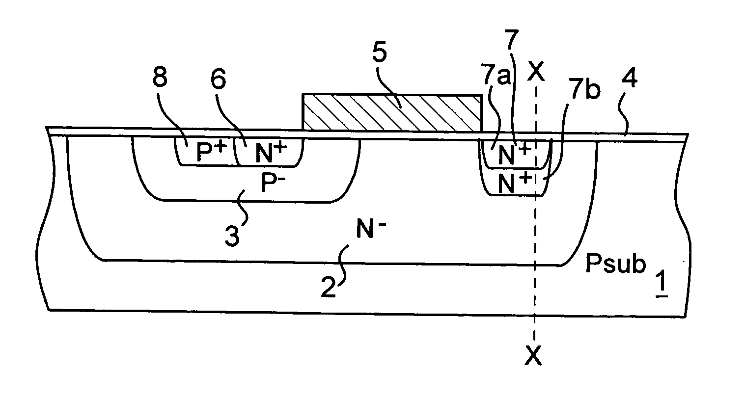
[0055]FIG. 1 shows a cross-sectional structure of a lateral double-diffused MOS transistor which is a first embodiment of the present invention. This lateral double-diffused MOS transistor is an N-channel type MOS transistor in this example and includes a lightly doped N-well diffusion region 2 serving as a drift region formed on a P-type substrate 1. A P-type body diffusion region 3 for forming a channel is formed on a surface within the lightly doped N-well diffusion region 102. A gate electrode 5 is provided in such a position as it covers from part of the P-body diffusion region 3 to part of the N-well diffusion region 2 located outside the diffusion region via gate oxide 4 serving as an insulating film. An N+ source diffusion region 6 and an N+ drain diffusion region 7 are formed on top of the P-body diffusion region 3 and top of the N-well diffusion region 2, respectively, both of which correspond to both sides of the gate electrode 5. A region of the P-body diffusion region 3...

second embodiment

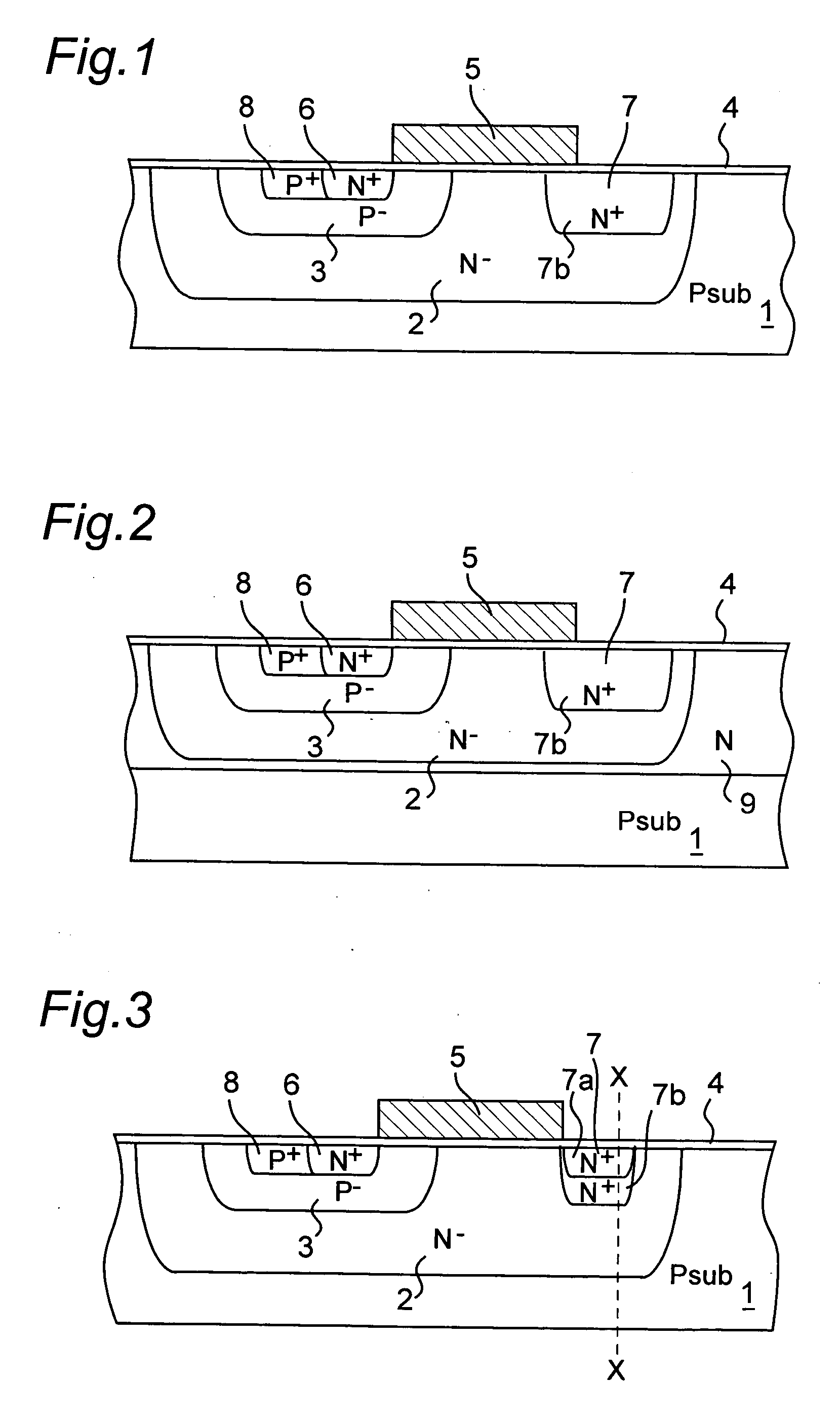
[0070]FIG. 2 shows a cross-sectional structure of a lateral double-diffused MOS transistor which is a second embodiment of the present invention. It is noted that component elements similar to those of FIG. 1 are designated by the same reference numerals. As in FIG. 1, interconnections, field film and overcoat film are omitted in illustration.

[0071] This lateral double-diffused MOS transistor differs from that of the first embodiment in that the MOS transistor is formed not in the P-type silicon substrate 1 but in an N-type epitaxial layer 9 formed on the P-type silicon substrate 1.

[0072] In some cases, MOS transistors are used in combination with bipolar transistors for improvement of their analog characteristic. In such a case, an N-type epitaxial layer 9 having a specified concentration may be formed on the P-type silicon substrate 1. In the example of FIG. 2, on top of such an N-type epitaxial layer 9 is formed an N-type drift region 2 having a concentration different from tha...

third embodiment

[0075]FIG. 3 shows a cross-sectional structure of a lateral double-diffused MOS transistor which is a third embodiment of the present invention. It is noted that component elements similar to those of FIG. 1 are designated by the same reference numerals. As in FIG. 1, interconnections, field film and overcoat film are omitted in illustration.

[0076] This lateral double-diffused MOS transistor differs from the first and second embodiments in that the drain diffusion region 7 is composed of two portions, a shallow diffusion portion 7a and a deep diffusion portion 7b, having different concentration distributions. The shallow diffusion portion 7a, which is formed shallow by using arsenic, is formed simultaneously with the source diffusion region 6 and in self alignment with the gate electrode 5. The deep diffusion portion 7b, which is formed deep by using phosphorus, has a 1 / 1000 or more concentration of the peak concentration of the source diffusion region 6 and is positioned deeper th...


PUM


Abstract

The lateral double-diffused MOS transistor includes a drift region of a first conductive type provided on a semiconductor substrate of a second conductive type, and a body diffusion region of the second conductive type formed on the surface within the drift region. The MOS transistor includes a gate electrode formed in such a position as it covers from part of the body diffusion region to part of the drift region located outside the diffusion region via an insulating film. The MOS transistor further includes a source diffusion region of the first conductive type and a drain diffusion region of the first conductive type formed on top of the body diffusion region and top of the drift region, respectively, both of which correspond to both sides of the gate electrode. The drain diffusion region includes a deep diffusion portion which has a 1 / 1000 or more concentration of a peak concentration of the source diffusion region and which is positioned deeper than the source diffusion region.

Description

CROSS-REFERENCE TO RELATED APPLICATION [0001] This Nonprovisional application claims priority under 35 U.S.C. §119(a) on Patent Application No(s). 2005-009993 filed in Japan on Jan. 18, 2005, the entire contents of which are hereby incorporated by reference. BACKGROUND OF THE INVENTION [0002] The present invention relates to a lateral double-diffused MOS transistor and a manufacturing method therefor. More particularly, the invention relates to a lateral double-diffused MOS transistor having high breakdown voltage and low on-state resistance characteristics as well as a manufacturing method therefor. [0003] In recent years, with the trend toward more multifunctional electronic equipment, semiconductor devices to be used therein have been diversified, confronting demands for higher breakdown-voltage, higher power, smaller size and lower power consumption. Achieving lower power consumption needs transistors of lower on-state resistance. [0004]FIG. 6 shows the structure of a common lat...

Claims


Application Information

Patent Timeline
Patent Type & Authority Applications(United States)
IPC IPC(8): H01L29/76
CPCH01L29/0873H01L29/0878H01L29/7816H01L21/18
Inventor TAKIMOTO, TAKAHIROFUKUSHIMA, TOSHIHIKO
Owner SHARP KK
Why Eureka
Try Eureka