
Nanophotonic integrated circuit and fabrication thereof

a nanophotonic integrated circuit and photonic technology, applied in the field of nanophotonic integrated circuits, can solve the problems of difficult external control, almost impossible to produce a true pic that can replicate the ic revolution, and inability to achieve a true integrated platform for fiberoptic communication and computing that can parallel the electronic counterpar

Inactive Publication Date: 2006-07-20
APPLIED RES & PHOTONICS
View PDF27 Cites 11 Cited by
  • Summary
  • Abstract
  • Description
  • Claims
  • Application Information

AI Technical Summary

Benefits of technology

[0020] An advantage of the present invention is the ability to provide a monolithically integrated, nanophotonic chip incorporating functionality for light guiding, light amplifying, light modulating, signal processing, attenuating, sensing, on-chip light source and detector, on-chip interconnect, and inputting and outputting of the signal, and combinations thereof.

Problems solved by technology

In the field of photonics, efforts to achieve a true integrated platform for fiberoptic communication and computing that can parallel the electronic counterpart have been unsuccessful.
This is primarily because silicon, as an optical material, poses several challenges that make it almost impossible to produce a true PIC that can replicate the IC revolution.
These issues are fundamental limitations that arise from material properties, and result in difficulty of externally controlling.
Silicon structures are difficult to control externally for optical switching.
Poor light emission from silicon devices is attributed to silicon's indirect band gap.
It is difficult to obtain optical amplification with silicon because of difficulty in doping silicon with amplifying ions.
It is also difficult to fabricate modulators because of silicon's low electro-optic coefficient.
On the other hand there exists a new set of challenges to overcome because of the difficulties with silicon material properties explained above, and because of the fact that silicon cannot do everything necessary for photon manipulations.
It is apparent that, while the term PIC has been used for a number of years, devices based on those PICs are not in wide use in practical network equipment.
The primary reason is the typical unfavorable cost and performance issues of the available PIC devices that need to be improved.
Also the above referenced PICs lack features to be able to term them as a complete PIC or an optical processor.

Method used


Image

  • Nanophotonic integrated circuit and fabrication thereof
  • Nanophotonic integrated circuit and fabrication thereof
  • Nanophotonic integrated circuit and fabrication thereof

Examples


Embodiment Construction

[0049] In the following description, reference is made to the accompanying drawings that form a part thereof, and in which is shown by way of illustration specific exemplary embodiments in which the invention can be practiced. These embodiments are described in sufficient detail to enable those skilled in the art to practice the invention. It is to be understood that other embodiments can be utilized and that changes can be made without departing from the scope of the present invention.

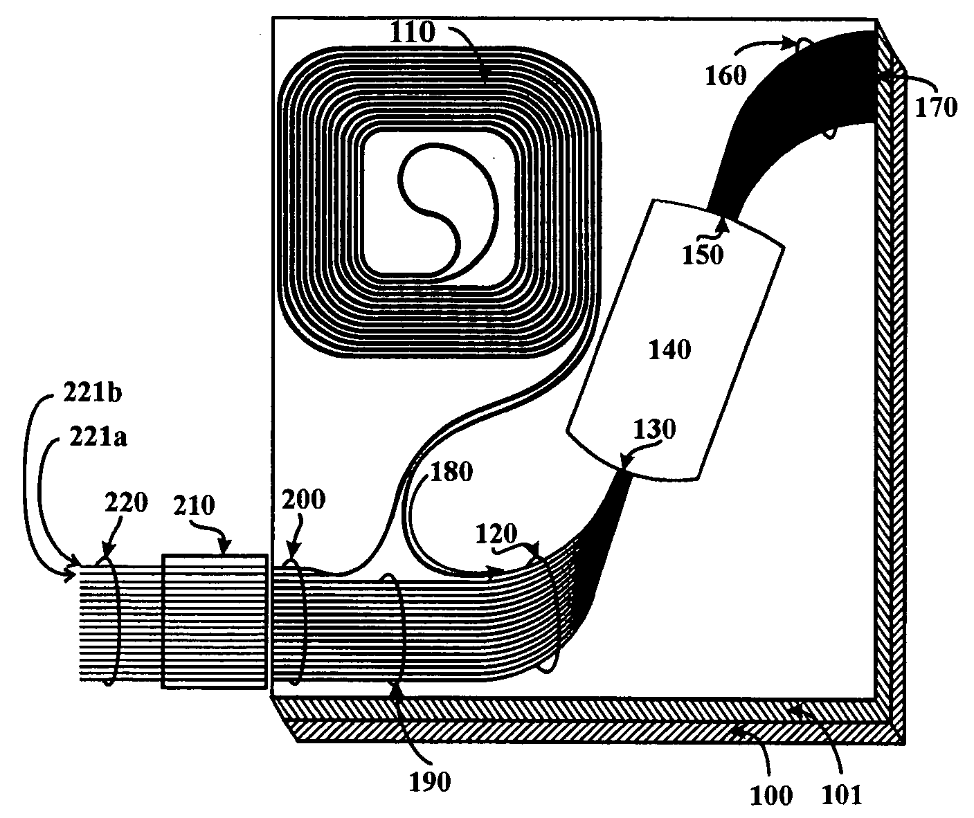
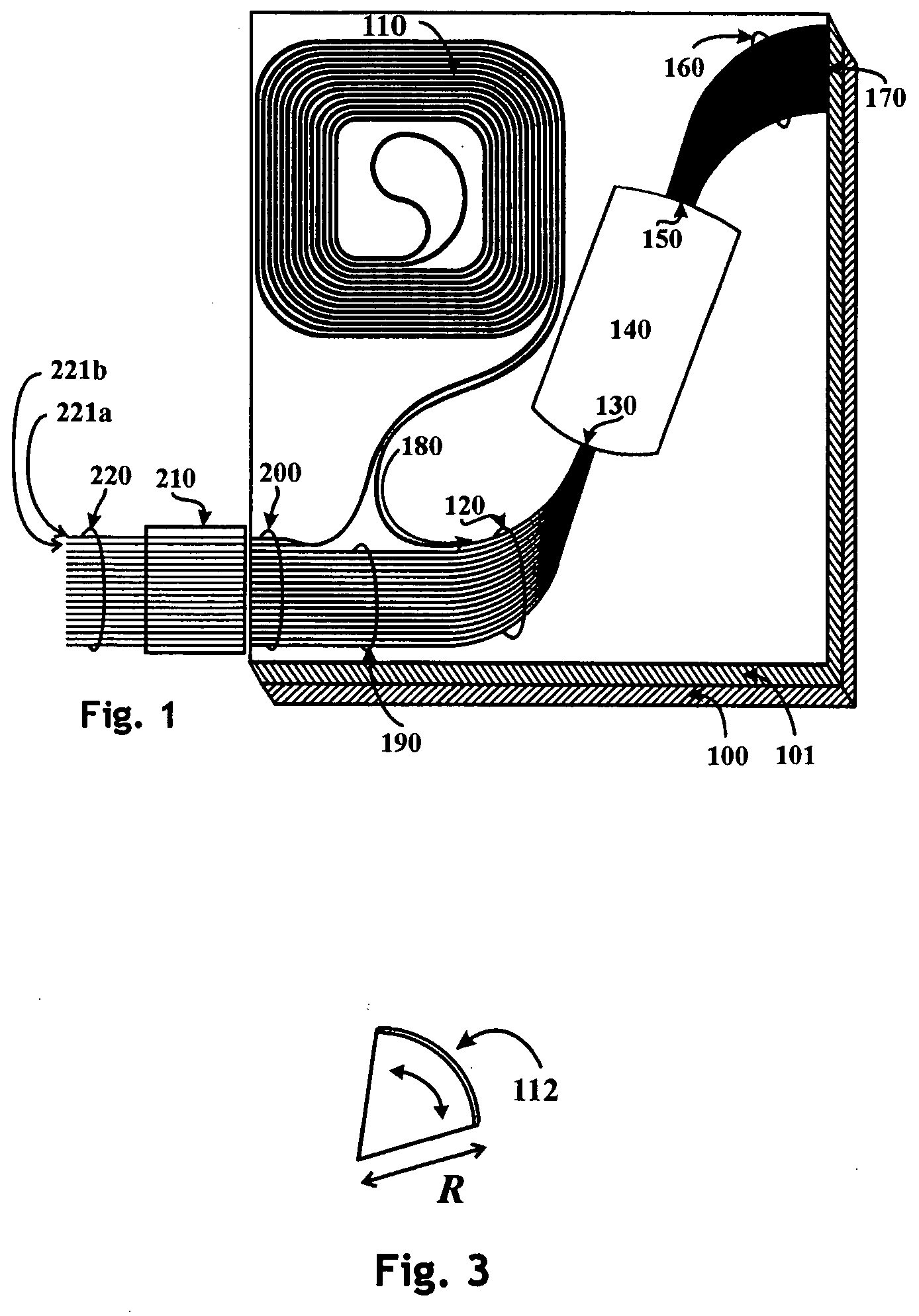
[0050]FIG. 1 provides a diagrammatic representation of the overall structure of a preferred embodiment of the nPIC. A substrate 100 is preferably made from prime grade silicon, on which a layer of oxide 101 is formed by either thermal oxidation or from a spin-on glass via spin coating and curing the subsequent film at a suitable temperature that may range from room temperature to a few hundreds of degrees of Celcius. Several photonic functionalities are provided via different segments: an amplifier ...


PUM


Abstract

A class of nanophotonic integrated circuit (nPIC) has been disclosed that is a platform technology for fiberoptic communication and computing, that is fabricated from waveguides that are based on natural index contrast (NIC) principle. A multifunctional nPIC and its fabrication details have been described. The nPIC is also known as an “optical processor”. A novel nanomaterial “dendrimer” is highlighted as the key ingredient that enables the fabrication of the nPICs and its multifunctionality from the same basic process. Other nanomaterials such as spin-on glass, nano-silica sol, and a combination of any of these materials can also be used via the natural index contrast method. Several preferred embodiments of the nPIC are described.

Description

CROSS-REFERENCE TO RELATED APPLICATIONS [0001] This application claims the benefit of U.S. Provisional Patent Application No. 60 / 593,508, filed Jan. 20, 2005 Nanophotonic Integrated Circuit: A Platform for an Optical Processor and Fabrication Thereof, which application is hereby incorporated by reference in its entirety. This application is related to U.S. patent application Ser. No. 10 / 605,638, filed Oct. 15, 2003, entitled Reflective Arrayed Waveguide Grating, which is hereby incorporated by reference in its entirety and assigned to the assignee of the present invention.FIELD OF THE INVENTION [0002] The present invention is directed to a nanophotonic integrated circuit and more particularly to a multifunctional nanophotonic integrated circuit (nPIC) and devices based on the nPIC. BACKGROUND OF THE INVENTION [0003] An integrated circuit (IC) is a microelectronic device that houses multiple electronic circuits on a chip. ICs are built by lithographic fabrication of numerous transist...

Claims


Application Information

Patent Timeline
Patent Type & Authority Applications(United States)
IPC IPC(8): H03K5/153
CPCG02B6/12011G02B6/1221H01S3/0637H01S3/1608H01S3/17
Inventor RAHMAN, ANIS
Owner APPLIED RES & PHOTONICS
Learn More