Method and apparatus for inspecting a defect of a pattern

a pattern and defect technology, applied in the field of pattern inspection, can solve the problems of local brightness differences across images, defect should not be detected as an essential defect, and reduce sensitivity, so as to achieve high sensitive, reduce brightness variations, and high pattern sensitive

Inactive Publication Date: 2006-07-20
HITACHI HIGH-TECH CORP
View PDF5 Cites 48 Cited by
  • Summary
  • Abstract
  • Description
  • Claims
  • Application Information

AI Technical Summary

Benefits of technology

[0010] Further, the present invention performs comparison inspections under multiple shiftable inspection conditions and then performs a comparison inspection through either integration of the inspection results or integration of images under different detection conditions, thereby implementing high sensitive pattern inspection capable of being applied to inspection for an increased variety of defects.
[0011] According to the present invention, a pattern inspection apparatus has a configuration that performs comparisons of images of regions corresponding to patterns formed to be same patterns and determines a mismatch portion to be a defect. In the configuration, high sensitive pattern inspection can be performed by reducing brightness variations across comparison images occurring in association with film thickness differences and pattern edge thickness differences, thereby enabling high sensitive pattern inspection capable of being applied to inspection for a large variety of defects.
[0012] Further, according to the present invention, in the pattern inspection apparatus, comparisons are performed under multiple shiftable inspection conditions, and either the results thereof are integrated or the comparison inspection is performed through integration of images under different detection conditions, thereby enabling high sensitive pattern inspection capable of being applied to inspection for a large variety of defects.
[0016] The configuration further includes means that extracts defect candidates through respective comparisons between the multiple same patterns and the defect candidates and that integrates the defect candidates extracted through the comparisons, thereby enabling sensitive defect detection even in the case that an inter-image brightness difference is occurring across the same patterns in association with a pattern linewidth difference.
[0018] The configuration further includes means of collecting and integrating statistical offset values, which are detected in a local region, from a wider region; and means of integrating the offset values with past different comparison inspections and detecting a final offset value to be a defect. Thereby, even when a large brightness difference is caused across specific inter-image patterns in association with an intra-wafer film thickness difference, such a difference can be restrained.
[0020] Further, according to the present invention, pattern images of a large number of chips formed on the wafer are separated into images in a chip comparison region and images in a cell comparison region, and image processes of a chip comparison and a cell comparison are parallel executed. Thereby, image detections with the stage movement can be completed in one time. Further, the throughput can be improved by combination with the parallel processing of the chip comparison and the cell comparison.

Problems solved by technology

In an inspection target semiconductor wafer, planarization by CMP (chemical mechanical polishing) or the like causes delicate differences in pattern film thickness, thereby causing local brightness differences across images of chips in association therewith.
However, such a defect should not be detected as an essential defect.
Such a detection result is caused in association with misreporting.
However, the method causes reduction in the sensitivity, so that a defect corresponding to a differential value of an equivalent level or lower cannot be detected.
According to the existing method of comparison inspection, when a brightness value variation such as described above is present across images of adjacent cells or adjacent chips, the variation appears as noise during the inspection.

Method used


Image

  • Method and apparatus for inspecting a defect of a pattern
  • Method and apparatus for inspecting a defect of a pattern
  • Method and apparatus for inspecting a defect of a pattern

Examples


Embodiment Construction

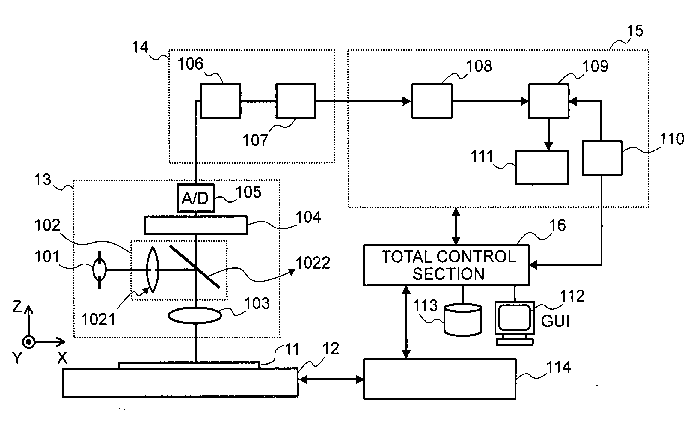
[0065] One embodiment of the present invention will be described below with reference to the drawings.

[0066] In addition, a pattern inspection apparatus according to the present embodiment includes imaging means that images optical images of patterns; storage means that stores multiple types of detection conditions of the optical images for being used by the imaging means to image the optical images of the patterns; and defect candidate extraction and classification means that sequentially detects the optical images of the patterns through the imaging means to thereby acquire multiple images different from one another in the detection condition by using the multiple types of detection conditions stored in the storage means and that extracts and classifies defect candidates by processing the multiple images different from one another in the detection condition.

[0067] In addition, a pattern inspection apparatus according to the present embodiment includes imaging means that images o...


PUM

PropertyMeasurementUnit
wavelengthaaaaaaaaaa
wavelengthsaaaaaaaaaa

Abstract

In a pattern inspection apparatus, influences of pattern brightness variations that is caused in association with, for example, a film thickness difference or a pattern width variation can be reduced, high sensitive pattern inspection can be implemented, and a variety of defects can be detected. Thereby, the pattern inspection apparatus adaptable to a broad range of processing steps is realized. In order to realize this, the pattern inspection apparatus of the present invention performs comparison between images of regions corresponding to patterns formed to be same patterns, thereby determining mismatch portions across the images to be defects. The apparatus includes multiple sensors capable of synchronously acquiring images of shiftable multiple detection systems different from one another, and an image comparator section corresponding thereto. In addition, the apparatus includes means of detecting a statistical offset value from the feature amount to be a defect, thereby enabling the defect to be properly detected even when a brightness difference is occurring in association with film a thickness difference in a wafer.

Description

BACKGROUND OF THE INVENTION [0001] The present invention relates to pattern inspection for detection of, for example, a defect and foreign matter by using an image of an object obtained in the manner that the object is irradiated with light or laser and is thereby imaged. More specifically, the invention relates to an apparatus and method for inspecting patterns (or, a “pattern inspection apparatus” and a “pattern inspection method”, hereafter) well suited for exterior inspection of, for example, semiconductor wafers, thin-film transistors (or, “TFTs,” hereafter), and photomasks. [0002] As an existing technology, a method of detecting a defect through comparison between an inspection targets image and a reference image is known, as is disclosed in, for example, in Japanese Unexamined Patent Application Publication No. 05-264467 (or, 1996-264467). [0003] According to this disclosed method, inspection target samples with repetitious patterns regularly arranged are serially imaged by a...

Claims


Application Information

Patent Timeline
Patent Type & Authority Applications(United States)
IPC IPC(8): G06K9/00G01N21/956G03F1/84G06T1/00H01L21/027H01L21/66
CPCG06T7/001G06T2207/30148G06T7/0004
Inventor SAKAI, KAORUMAEDA, SHUNJISHIBUYA, HISAENISHIYAMA, HIDETOSHI
Owner HITACHI HIGH-TECH CORP
Why Eureka
Try Eureka