Multi-junction, monolithic solar cell with active silicon substrate

a solar cell and active silicon technology, applied in the direction of photovoltaics, electrical devices, semiconductor devices, etc., can solve the problems of reducing the overall efficiency of the pv cell to convert radiant energy into electrical energy, positional errors, and difficult economic collection, storage and transportation of solar energy

Inactive Publication Date: 2006-07-27
ALLIANCE FOR SUSTAINABLE ENERGY
View PDF10 Cites 66 Cited by
  • Summary
  • Abstract
  • Description
  • Claims
  • Application Information

AI Technical Summary

Benefits of technology

[0014] In accordance with a first embodiment of the present invention, a two-subcell PV cell includes a compliant silicon substrate having a first PV subcell formed therein, upon which is epitaxially grown a second PV subcell. In this embodiment, the second PV subcell is formed of a Group III-V direct bandgap semiconductor material having a lattice constant that is flexibly accommodated by the compliant silicon substrate. The compliant silicon substrate includes a silicon base layer, a conductive perovskite layer, and a Silicon Dioxide (SiO2) layer formed between the silicon base layer and the conductive perovskite layer. In this embodiment, the first PV subcell is formed within the base silicon layer and the conductive perovskite layer allows for the conduction of charge carriers between the first and second PV subcells.

Problems solved by technology

Despite this abundance, solar energy has proven difficult to economically collect, store, and transport, and, thus has been relatively overlooked compared to the other more conventional energy sources, i.e., oil, gas and coal.
Non-monolithic PV cells require the mechanical alignment and adhesion between different subcells in the cell, a process that is time consuming, costly and can lead to positional errors not evident in monolithic cells.
A limitation in designing multi-junction, monolithic PV cells, particularly PV cells having layers formed from Group III-V direct band-gap semiconductor materials, is the desire for lattice matching between adjacently stacked layers of semiconductor materials that make-up the multi-subcells of the PV cell.
Lattice mismatching between adjacent layers of a PV cell results in strain and dislocations to form, thereby reducing the overall efficiency of the PV cell to convert radiant energy into electrical energy.
However, there is a limited selection of known Group III-V direct band-gap semiconductor materials having the requisite band-gap energies for use in a PV cell, and of these only a few can be lattice matched to form a monolithic PV cell.
Lattice matching limitations between Group III-V direct band-gap semiconductor materials is further exacerbated by the fact that the PV subcell semiconductor material is grown on a substrate template, where the substrate has its own, and ultimately limiting, lattice constant that must be matched.
As such, the design of monolithic PV cells using Group III-V semiconductor materials are typically limited to a set of defined substrate / semiconductor materials having matched lattice constants and appropriate band-gap energy for the intended use.
While silicon would be an ideal substrate in terms of durability and expense for use in PV cells, silicon has a lattice constant that is incompatible with most Group III-V direct band-gap semiconductor materials.
One obstacle to fabrication and design of such series-connected multi-subcell PV cells is that the STO layer acts as an electric insulator blocking the flow of charge carriers between the silicon base layer and the PV subcell(s) formed on the compliant substrate.

Method used


Image

  • Multi-junction, monolithic solar cell with active silicon substrate
  • Multi-junction, monolithic solar cell with active silicon substrate
  • Multi-junction, monolithic solar cell with active silicon substrate

Examples


first embodiment

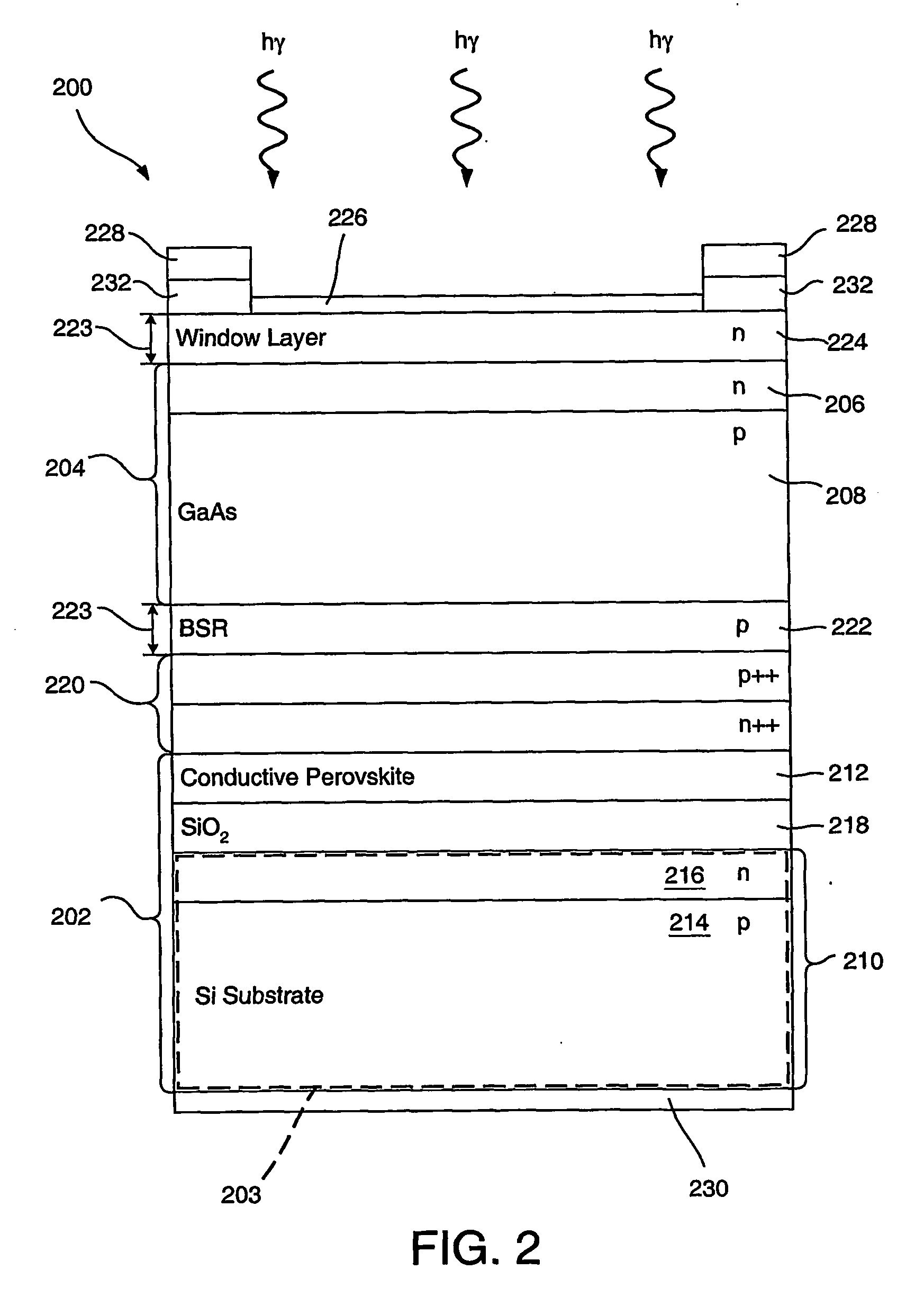
[0039]FIG. 2 illustrates a two subcell, tandem monolithic photovoltaic (PV) cell 200 in accordance with the present invention. As shown, the PV cell 200 generally includes, a compliant silicon substrate 202, having formed therein a first PV subcell 203, and a second PV subcell 204. Both the first PV subcell 203 and a second PV subcell 204 are operable to produce a photocurrent when photons having appropriate energy levels impinge on them.

[0040] The compliant silicon substrate 202 is generally composed of a base silicon layer 210 and a conductive perovskite layer 212. The base silicon layer 210 is composed substantially of silicon that has been doped (e.g., impurities added that accept or donate electrons) to form appropriate p-type 214 and n-type 216 regions of the first PV subcell 203. The base silicon layer 210 preferably has a band-gap energy of approximately 1.1 eV. In one embodiment, the conductive perovskite layer 212 comprises Strontium Titanate (SrTiO3) that has been electro...

second embodiment

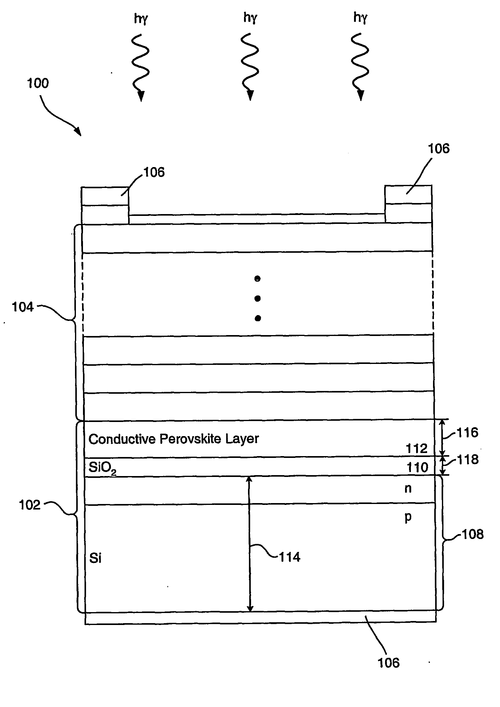
[0049] Turning now to FIG. 3, illustrated therein is a three-PV subcell, tandem monolithic PV cell 300 in accordance with the present invention. As shown, the PV cell 300 generally includes, a compliant silicon substrate 302, having formed therein a first PV subcell 303, a second PV subcell 304, and a third PV subcell 305. The first PV subcell 303, the second PV subcell 304, and the third PV subcell 305 are all preferably operable to produce a photocurrent when photons having appropriate energy levels impinge on them.

[0050] The compliant silicon substrate 302 is generally composed of a base silicon layer 310, an intermediary oxide layer 318, and a conductive perovskite layer 312. The base silicon layer 310 is composed substantially of silicon that has been doped (e.g., impurities added that accept or donate electrons) to form appropriate p-type 314 and n-type 316 regions of the first PV subcell 303. The base silicon layer 310 preferably has a band-gap energy of approximately 1.1 eV....


PUM


Abstract

A monolithic multi-junction (tandem) photo-voltaic (PV) device includes one or more PV subcells epitaxially formed on a compliant silicon substrate (102). The compliant silicon substrate (102) includes a base silicon layer (108), a conductive perovskite layer (112), and an oxide layer (110) interposed between the base silicon layer (108) and the conductive perovskite layer (112). A PV subcell is formed within the base silicon layer (108) of the conductive silicon substrate (102). The conductive perovskite layer (112) facilitates the conduction of charge carriers between the PV subcell formed in the compliant silicon substrate (102) and the one or more PV subcells formed on the compliant silicon substrate (102).

Description

CONTRACTUAL ORIGIN OF THE INVENTION [0001] The United States Government has rights in this invention under Contract No. DE-AC36-99GO10337 between the United States Department of Energy and the National Renewable Energy Laboratory, a Division of the Midwest Research Institute.TECHNICAL FIELD [0002] The present invention relates generally to energy conversion devices, and more particularly to series-connected, monolithic tandem PV cells having one or more PV subcells formed on a compliant silicon substrate, wherein the compliant silicon substrate includes a PV subcell formed therein. BACKGROUND ART [0003] Solar energy represents a vast source of non-polluting, harnessable energy. It is estimated that the amount of solar energy striking the United States each year far exceeds the country's energy needs for that year. Despite this abundance, solar energy has proven difficult to economically collect, store, and transport, and, thus has been relatively overlooked compared to the other mor...

Claims


Application Information

Patent Timeline
Patent Type & Authority Applications(United States)
IPC IPC(8): H01L31/00
CPCH01L31/03046H01L31/0687H01L31/1852Y02E10/544
Inventor MASCARENHAS, ANGELOSEONG, MAENG-JE
Owner ALLIANCE FOR SUSTAINABLE ENERGY
Why Eureka
Try Eureka