Vertical MOSFET with dual work function materials

a work function material and vertical pass transistor technology, applied in the field of vertical pass transistors, can solve the problems of low carrier mobility, high junction leakage, and low retention time, and achieve the effect of adequate write back current and suppression of all leakage current components

Inactive Publication Date: 2006-07-27
GLOBALFOUNDRIES INC
View PDF2 Cites 38 Cited by
  • Summary
  • Abstract
  • Description
  • Claims
  • Application Information

AI Technical Summary

Benefits of technology

[0015] It is yet another object to provide a method for optimizing the work function material for a vertical transistor in a DRAM cell in terms of its effect on the threshold voltage.
[0016] It is still another object to suppress all leakage current components and maintain an adequate write back current in the vertical DRAM pass transistor.

Problems solved by technology

Increasing channel doping results in a degraded retention time due to junction leakage.
With N+ polysilicon used as gate material, a high channel doping must be used to achieve a high Vt while the high channel doping can lead to high junction leakage, low carrier mobility and high back bias sensitivity.
Therefore, it becomes a challenge to prevent the three previously mentioned leakages and still maintain an appropriate write back current.
There are still others disadvantages regarding this method.
First, there remains a large body effect for the device which degrades the write back current.
Second, the Vt adjustment implant cannot be totally decoupled from the doping near the storage node as a result of the diffusion of the channel dopant being boron.
The difficulty of this design is that Vt of the device is highly sensitive to the deep trench top recess depth which, from a process point of view, is difficult to control.
While the negative wordline voltage causes a large gate induced drain leakage (GIDL) current and degrades the retention performance, having a negative wordline voltage in a DRAM pass gate is not possible.

Method used


Image

  • Vertical MOSFET with dual work function materials
  • Vertical MOSFET with dual work function materials
  • Vertical MOSFET with dual work function materials

Examples


Embodiment Construction

[0030] The present invention described a vertical DRAM pass transistor having two different gate work function materials and a method of fabrication thereof.

[0031] In a first embodiment, N+ doped polysilicon is used for the gate near the storage node. Above the N+ gate polysilicon, another gate material with a higher work function, such as silicide, is used to control Vt for the transistor. The metal and silicide gate materials with higher work function that can be advantageously used as dual work function gate materials, according to the present invention, are shown in Table I.

TABLE IMetalWorkfunction (V)SilicideWorkfunction (V)Al4.71-4.81CrSi24.64Au4.9MoSi24.62Cr4.65NiSi24.72Mo4.65Pd2Si24.78Ti4.57PtSi4.9W4.67TiSi24.65WSi24.7

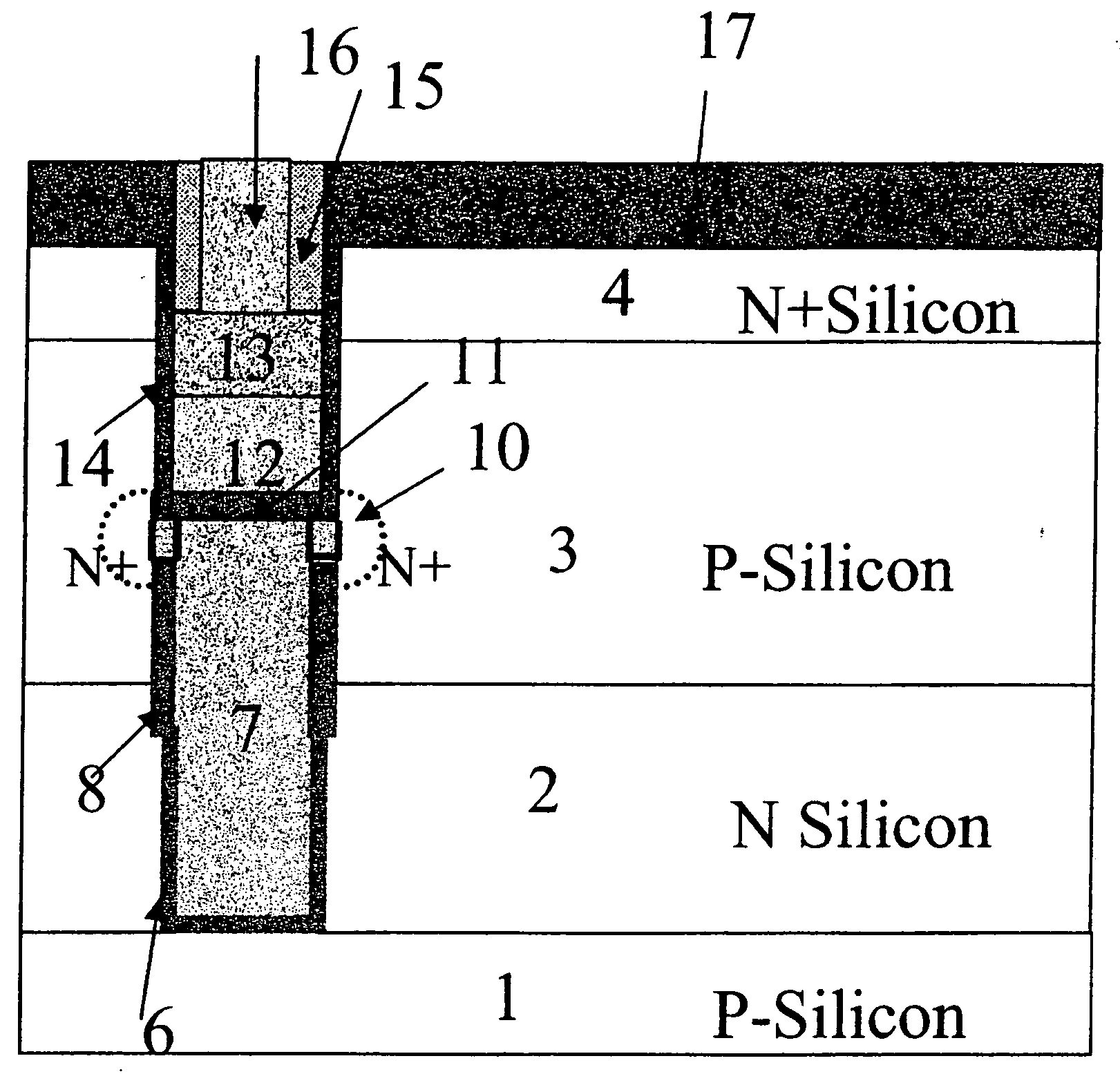
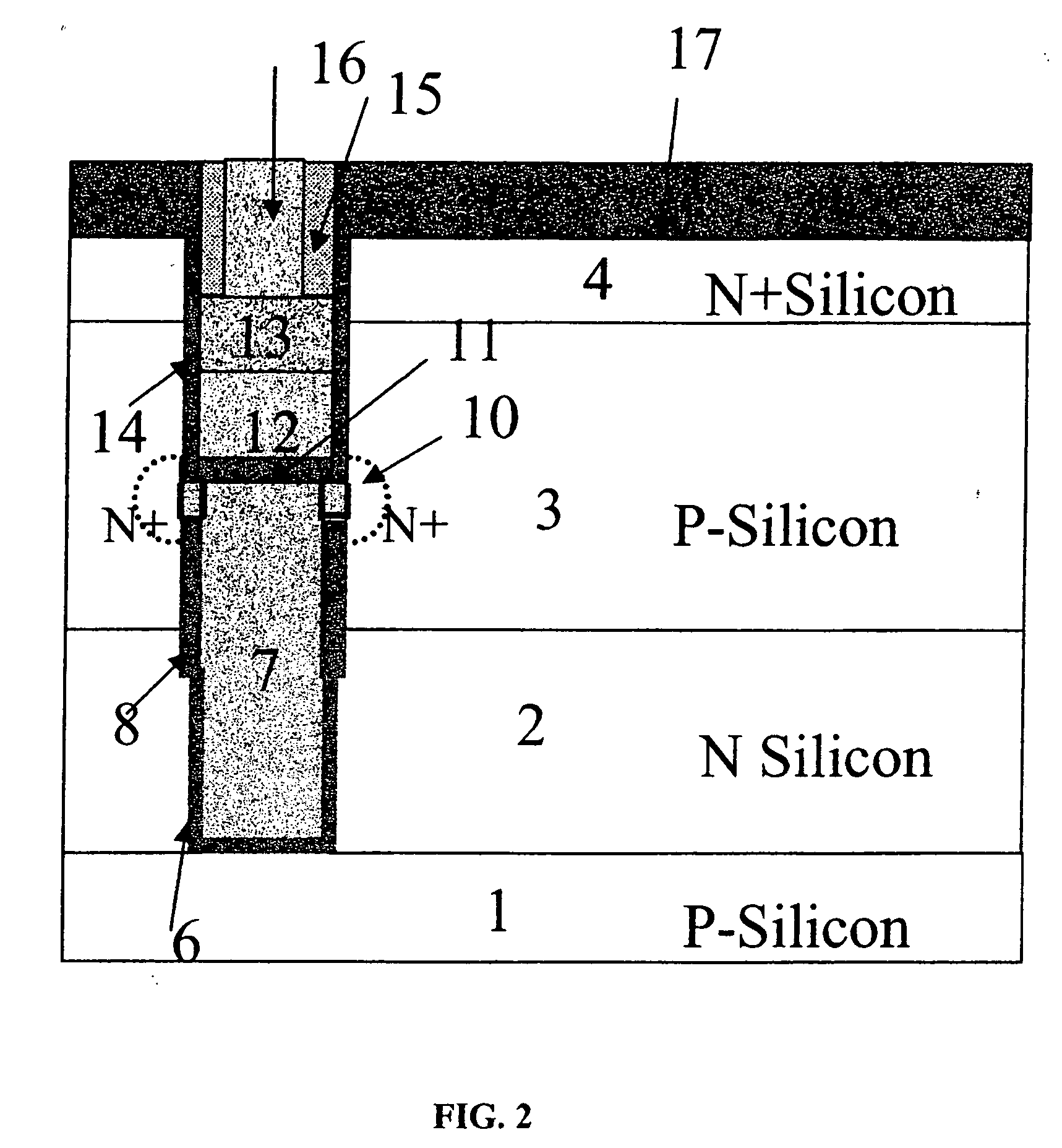
[0032] Referring now to FIG. 2, there is shown a cross-section view of the vertical pass transistor at the DRAM storage node. The vertical pass transistor is fabricated coupled to a deep trench capacitor, with source 4 and drain 10 separated by a channel reg...


PUM


Abstract

A vertical pass transistor used in a DRAM cell for maintaining a low total leakage current and providing adequate drive current is described together with a method of fabricating such a device. The transistor gate is engineered in lieu of the channel. The vertical pass transistor for the DRAM cell incorporates two gate materials having different work functions. The gate material near the storage node is n-type doped polysilicon. The gate material near the bit line diffusion is made of silicide or metal having a higher work function than the n-polysilicon. The novel device structure shows several advantages: the channel doping is reduced while maintaining a high Vt and a low sub-threshold leakage current; the carrier mobility improves with the reduced channel doping; the body effect of the device is reduced which improves the write back current; and the sub-threshold swing is reduced because of the low channel doping.

Description

BACKGROUND OF THE INVENTION [0001] This invention relates to semiconductor transistors, and more particularly, to a vertical pass transistor having a gate with dual work function materials for use in Dynamic Random-Access Memory (DRAM) cell applications. [0002] DRAM pass transistors require off-state leakage current of less than 1 fA per cell to achieve an adequate retention time. The scaling of channel length requires higher channel doping to control short channel effect and sub-threshold leakage. Increasing channel doping results in a degraded retention time due to junction leakage. These and other constraints present a challenge when designing planar pass transistor at below 100 nm node, as described in an article by J. Mandelman et al., “Challenges and future directions for the scaling of dynamic random-access memory (DRAM),” IBM Journal of Research and Development, Vol. 46, (2002), pp.187-213. A vertical pass transistor coupled to a deep trench capacitor cell design is an alter...

Claims


Application Information

Patent Timeline
Patent Type & Authority Applications(United States)
IPC IPC(8): H01L29/94
CPCH01L27/10864H01L29/66181H10B12/0383
Inventor CHEN, XIANGDONGWANG, GENGLI, YUJUNOUYANG, QIQING C.
Owner GLOBALFOUNDRIES INC
Why Eureka
Try Eureka