Insulated gate semiconductor device and method of manufacturing the same

a technology of semiconductor devices and semiconductor devices, which is applied in the direction of semiconductor devices, basic electric elements, electrical equipment, etc., can solve the problems of power device loss, steady state loss, switching loss caused,

Active Publication Date: 2006-07-27
FUJI ELECTRIC CO LTD
View PDF9 Cites 25 Cited by
  • Summary
  • Abstract
  • Description
  • Claims
  • Application Information

AI Technical Summary

Benefits of technology

[0012] Portions of the second semiconductor layer extending between the adjacent trenches are covered with an insulator layer between the adjacent third semiconductor regions. The third semiconductor regions and the fourth semiconductor region(s) can be connected electrically to each other through the common portions of the emitter electrode. The third semiconductor regions can be aligned diagonally to the trenches such that a checkered pattern is formed. The trenches can be arranged at an equal interval and-the width W of the regions sandwiched between the trenches can satisfy the following condition W<0.186V1 / 2, where V represents the rated voltage of the insulated gate semiconductor device. The ratio of the sum of the surface areas of the third semiconductor regions and the fourth semiconductor region to the surface area of the first semiconductor layer can be 80% or lower and 10% or higher, namely between 10-80%.

Problems solved by technology

The losses in the power device include the steady state losses determined by the ON-state voltage drop and the switching losses caused by the ON-OFF operations.
It is essentially difficult for the structure shown in FIG. 14 to obtain a high breakdown voltage.

Method used


Image

  • Insulated gate semiconductor device and method of manufacturing the same
  • Insulated gate semiconductor device and method of manufacturing the same
  • Insulated gate semiconductor device and method of manufacturing the same

Examples


Embodiment Construction

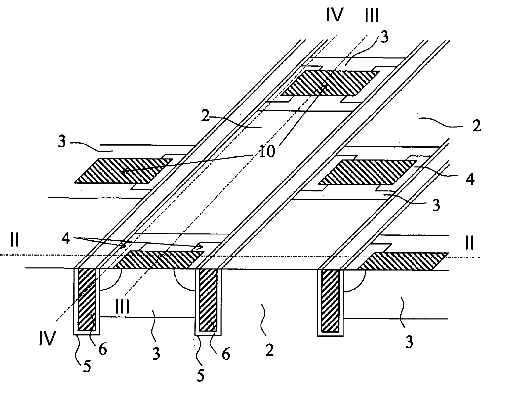
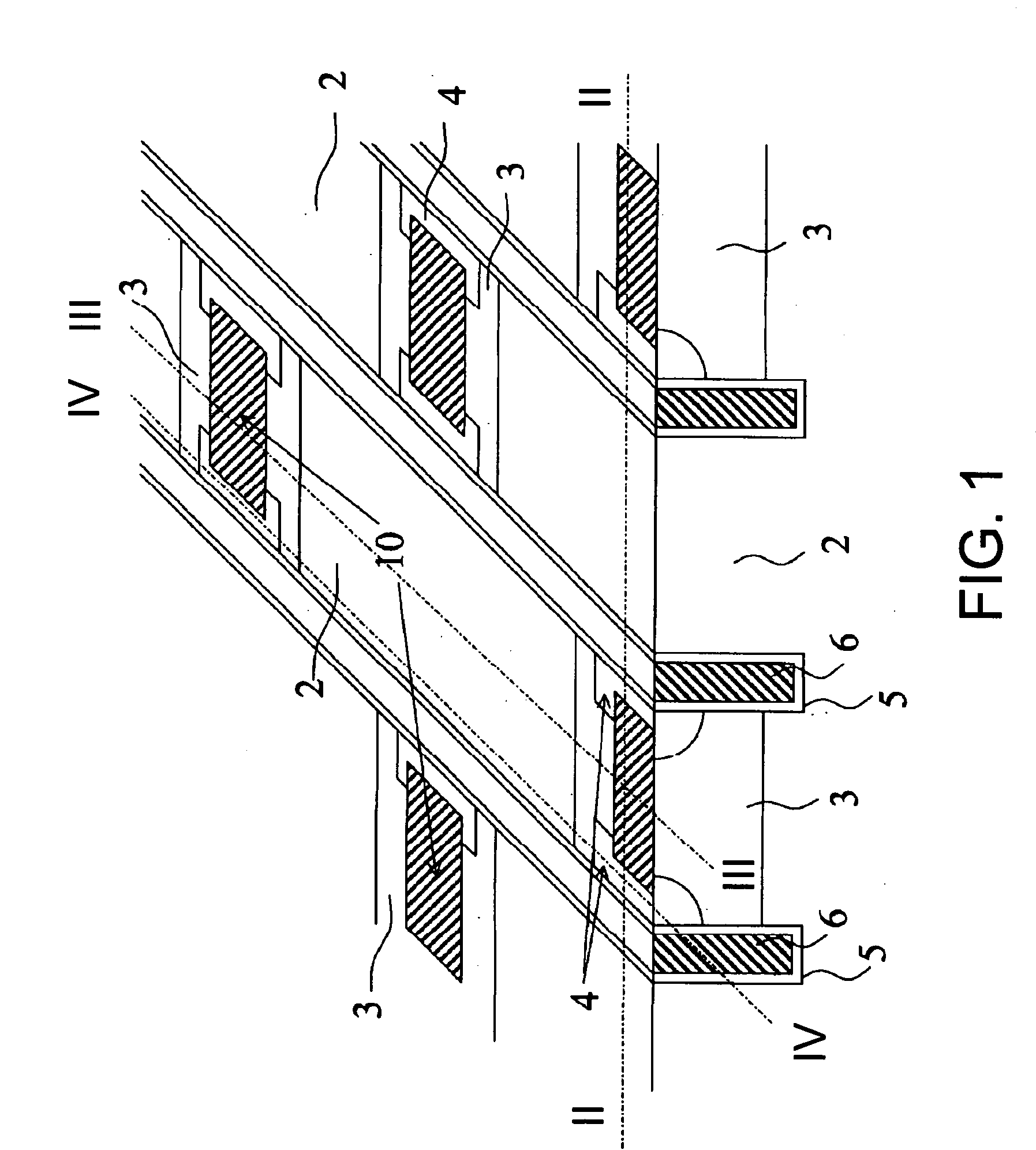
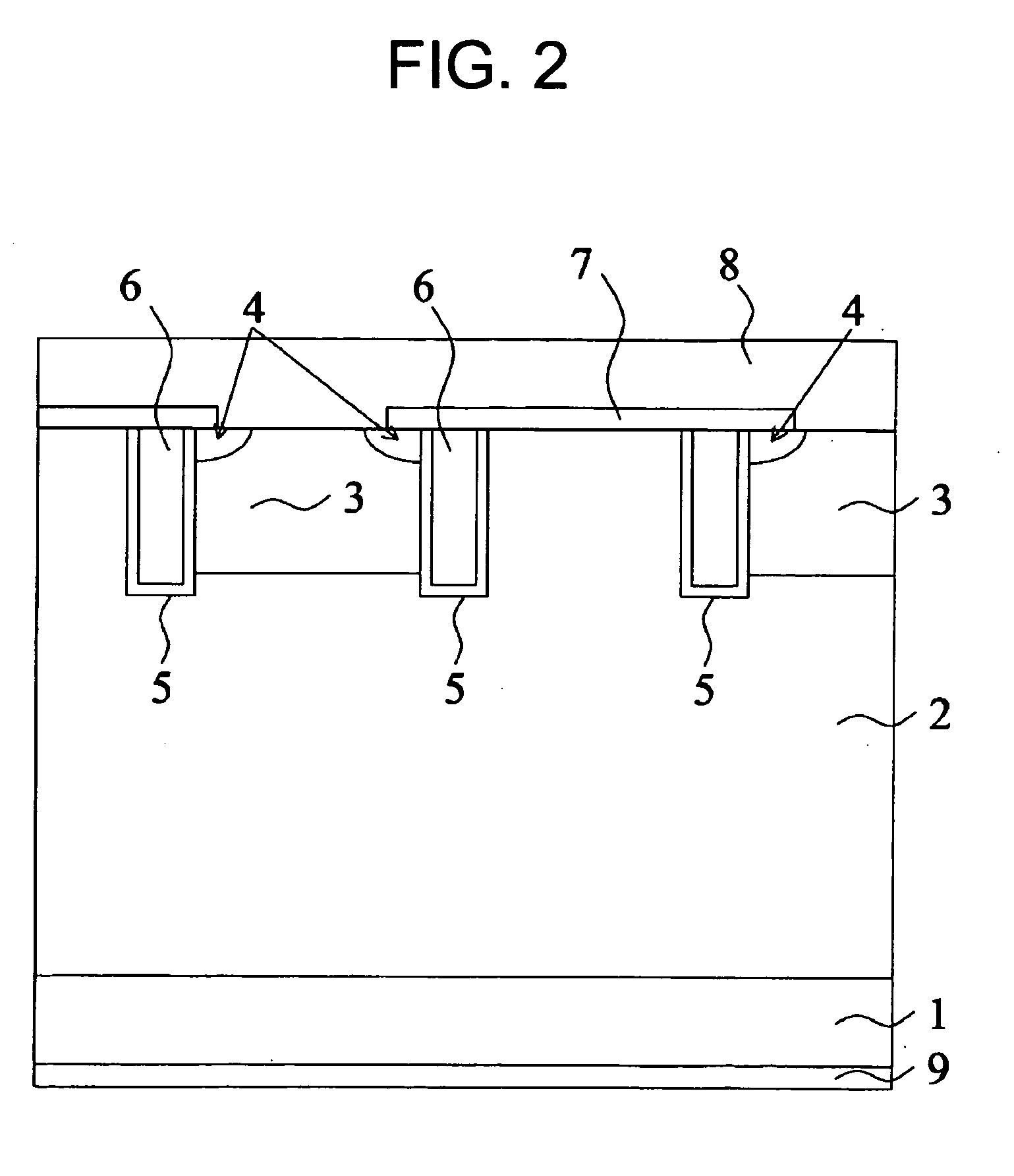
[0029] To obviate the problems described above, the surface structure for a vertical IGBT is provided with the following three specific features. First, for improving the turn-on characteristics, the mesa region potential is fixed by connecting the mesa regions sandwiched between the trenches to the emitter electrode so that the mesa regions is not floating. Note that the mesa region corresponds to the p-type base region between the trenches or the portion of the n-type drift layer extending between the trenches. The Yamaguchi publication describes that the floating mesa region potential varies the gate potential in the turn-on process, destabilizing the turn-on operations of the IGBT and impairing the controllability of the IGBT. Therefore, the turn-on characteristics can be improved essentially by removing the floating regions. If the floating regions, however, are simply eliminated, the structure will return to the typical trench IGBT, loosing the IE effects and increasing the ON...


PUM


Abstract

A trench MOSFET includes mesa regions between the trenches. The mesa regions are connected to an emitter electrode to fix the mesa region potential so that the mesa regions do not form a floating structure. P-type base regions are distributed in the mesa regions, and the distributed p-type base regions (e.g., the limited regions in the mesa regions) are provided with an emitter structure. The trench MOSFET can lower the switching losses, reducing the total losses while suppressing the ON-state voltage drop of the trench IGBT as low as the ON-state voltage drop of the IEGT, and improving the turn-on characteristics thereof. The trench MOSFET also can reduce the capacitance between the gates and the emitter thereof, since the regions where the gate electrode faces the emitter structure are reduced. The trench MOSFET can have trench gate structures set at a narrow interval to relax the electric field localization to the bottom portions of the trenches and obtain a high breakdown voltage. The trench MOSFET narrows the mesa region width between the trenches such that the portions of the n-type layer in the mesa regions extending between the trenches are depleted easily by applying a voltage of around several volts.

Description

BACKGROUND [0001] In exploring the developments of electric power converters that exhibit lower electric power consumption, power devices that play a key role in the electric power converters have been expected to exhibit a lower electric power consumption. Among the power devices, insulated gate bipolar transistors (hereinafter referred to as “IGBTs”) have been popular because the IGBTs can achieve a low ON-state voltage drop due their conductivity modulation effects and can be driven easily via their gate controlled with a voltage applied thereto. In particular, trench IGBTs, which have a trench structure including trenches formed from the wafer surface and gate electrodes buried in the respective trenches with an oxide film interposed between the gate electrode and the trench wall, are now becoming more popular. Since channels are formed on both sides of each trench, the trench IGBT increases the channel density and lowers the ON-state voltage drop thereof as compared with the so...

Claims


Application Information

Patent Timeline
Patent Type & Authority Applications(United States)
IPC IPC(8): H01L29/94
CPCH01L29/0696H01L29/7397
Inventor OTSUKI, MASAHITO
Owner FUJI ELECTRIC CO LTD
Why Eureka
Try Eureka